|
|
PDF P0327WC12E Data sheet ( Hoja de datos )
| Número de pieza | P0327WC12E | |
| Descripción | Fast Turn-off Thyristor | |
| Fabricantes | IXYS | |
| Logotipo |  |
|
Hay una vista previa y un enlace de descarga de P0327WC12E (archivo pdf) en la parte inferior de esta página. Total 12 Páginas | ||
|
No Preview Available !
Date:- 07 August 2012
Data Sheet Issue:- K1
Fast Turn-off Thyristor
Types P0327WC08# & P0327WC12#
Absolute Maximum Ratings
VDRM
VDSM
VRRM
VRSM
VOLTAGE RATINGS
Repetitive peak off-state voltage, (note 1)
Non-repetitive peak off-state voltage, (note 1)
Repetitive peak reverse voltage, (note 1)
Non-repetitive peak reverse voltage, (note 1)
MAXIMUM
LIMITS
800-1200
800-1200
800-1200
900-1300
UNITS
V
V
V
V
IT(AV)
IT(AV)
IT(RMS)
IT(d.c.)
ITSM
ITSM2
I2t
I2t
(di/dt)cr
VFGM
IFGM
VRGM
PG(AV)
PGM
VGD
THS
Tstg
OTHER RATINGS
Mean on-state current, Tsink=55°C, (note 2)
Mean on-state current. Tsink=85°C, (note 2)
Nominal RMS on-state current, Tsink=25°C, (note 2)
D.C. on-state current, Tsink=25°C, (note 4)
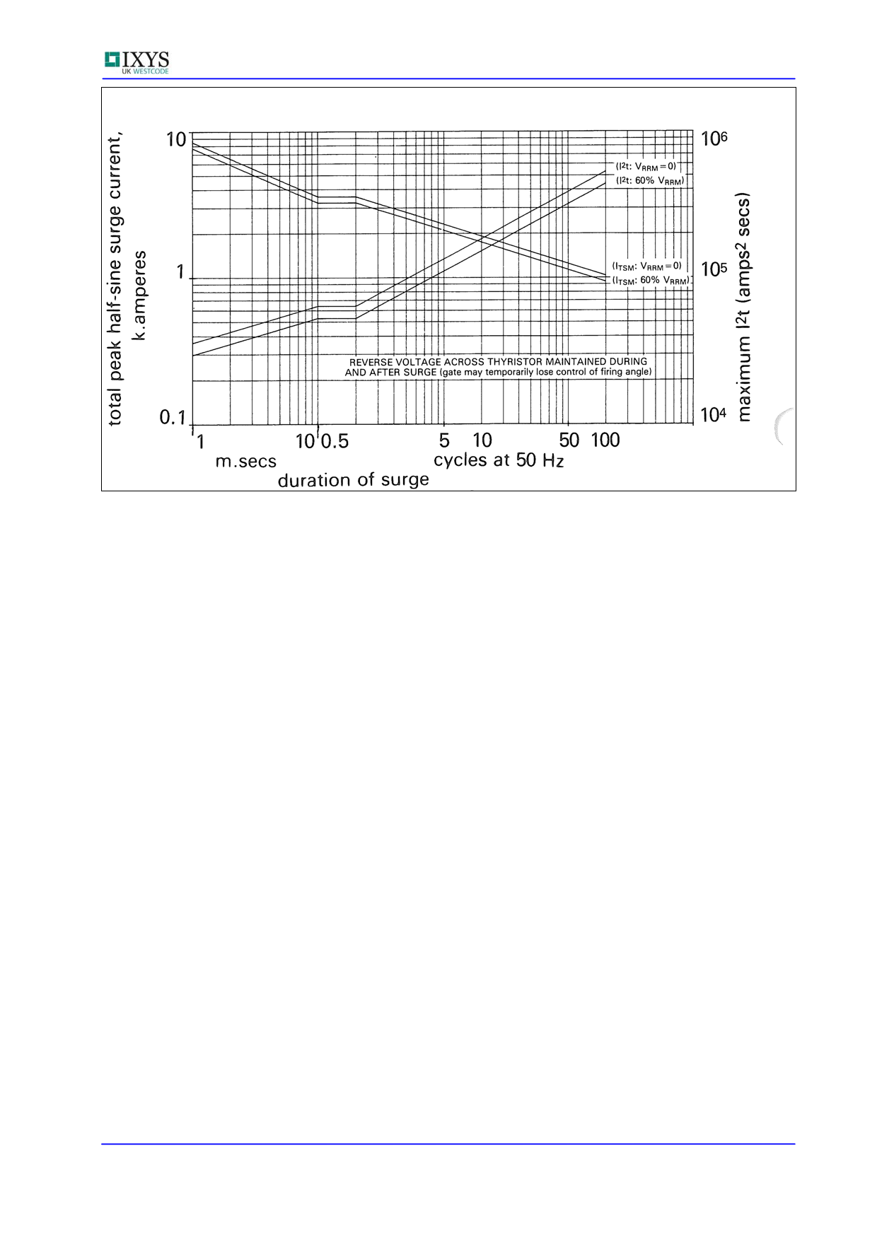
Peak non-repetitive surge tp=10ms, VRM=0.6VRRM, (note 5)
Peak non-repetitive surge tp=10ms, VRM≤10V, (note 5)
I2t capacity for fusing tp=10ms, VRM=0.6VRRM, (note 5)
I2t capacity for fusing tp=10ms, VRM≤10V, (note 5)
Maximum rate of rise of on-state current (repetitive), (Note 6)
Maximum rate of rise of on-state current (non-repetitive), (Note 6)
Peak forward gate voltage
Peak forward gate current
Peak reverse gate voltage
Mean forward gate power
Peak forward gate power (100µs pulse width)
Non-trigger gate voltage, (Note 7)
Operating temperature range
Storage temperature range
Notes:-
1) De-rating factor of 0.13% per °C is applicable for Tj below 25°C.
2) Double side cooled, single phase; 50Hz, 180° half-sinewave.
3) Single side cooled, single phase; 50Hz, 180° half-sinewave.
4) Double side cooled.
5) Half-sinewave, 125°C Tj initial.
6) VD=80% VDRM, IFG=1A, tr≤1µs, Tcase=125°C.
7) Rated VDRM.
MAXIMUM
LIMITS
330
120
670
525
3250
3575
63.9×1033
47×103
500
1000
12
18
5
1.5
60
0.25
-40 to +125
-40 to +150
UNITS
A
A
A
A
A
A
A2s
A2s
A/µs
A/µs
V
A
V
W
W
V
°C
°C
Data Sheet. Types P0327WC08# to P0327WC12# Issue K1
Page 1 of 12
August 2012
1 page 
Fast turn-off thyristor types P0327WC08# & P0327WC12#
The total dissipation is now given by:
W(TOT) = W (original) + E ⋅ f
12.2 Determination without Measurement
In circumstances where it is not possible to measure voltage and current conditions, or for design
purposes, the additional losses E in joules may be estimated as follows.
Let E be the value of energy per reverse cycle in joules (curves in Figure 9).
Let f be the operating frequency in Hz
( )TSINK (new) = TSINK (original ) − E ⋅ Rth ⋅ f
Where TSINK (new) is the required maximum heat sink temperature and
TSINK (original) is the heat sink temperature given with the frequency ratings.
A suitable R-C snubber network is connected across the thyristor to restrict the transient reverse voltage
to a peak value (Vrm) of 67% of the maximum grade. If a different grade is being used or Vrm is other than
67% of Grade, the reverse loss may be approximated by a pro rata adjustment of the maximum value
obtained from the curves.
12.3 Reverse Recovery Loss by Measurement
This thyristor has a low reverse recovered charge and peak reverse recovery current. When measuring
the charge care must be taken to ensure that:
(a) a.c. coupled devices such as current transformers are not affected by prior passage of high
amplitude forward current.
(b) A suitable, polarised, clipping circuit must be connected to the input of the measuring oscilloscope
to avoid overloading the internal amplifiers by the relatively high amplitude forward current signal
(c) Measurement of reverse recovery waveform should be carried out with an appropriate critically
damped snubber, connected across diode anode to cathode. The formula used for the calculation
of this snubber is shown below:
R2 = 4 ⋅ Vr
CS
⋅ di
dt
Where: Vr = Commutating source voltage
CS = Snubber capacitance
R = Snubber resistance
13.0 Gate Drive
The recommended pulse gate drive is 20V, 20Ω with a short-circuit current rise time of not more than
1µs. This gate drive must be applied when using the full di/dt capability of the device.
The duration of pulse may need to be configured with respect to the application but should be no shorter
than 20µs, otherwise an increase in pulse current could be needed to supply the resulting increase in
charge to trigger.
Data Sheet. Types P0327WC08# to P0327WC12# Issue K1
Page 5 of 12
August 2012
5 Page 
Fast turn-off thyristor types P0327WC08# & P0327WC12#
Data Sheet. Types P0327WC08# to P0327WC12# Issue K1
Page 11 of 12
August 2012
11 Page | ||
| Páginas | Total 12 Páginas | |
| PDF Descargar | [ Datasheet P0327WC12E.PDF ] | |
Hoja de datos destacado
| Número de pieza | Descripción | Fabricantes |
| P0327WC12C | Fast Turn-off Thyristor | IXYS |
| P0327WC12D | Fast Turn-off Thyristor | IXYS |
| P0327WC12E | Fast Turn-off Thyristor | IXYS |
| P0327WC12F | Fast Turn-off Thyristor | IXYS |
| Número de pieza | Descripción | Fabricantes |
| SLA6805M | High Voltage 3 phase Motor Driver IC. |
Sanken |
| SDC1742 | 12- and 14-Bit Hybrid Synchro / Resolver-to-Digital Converters. |
Analog Devices |
|
DataSheet.es es una pagina web que funciona como un repositorio de manuales o hoja de datos de muchos de los productos más populares, |
| DataSheet.es | 2020 | Privacy Policy | Contacto | Buscar |
