|
|
|
PDF AT45DB041B Data sheet ( Hoja de datos )
| Número de pieza | AT45DB041B | |
| Descripción | 4-megabit 2.5-volt Only or 2.7-volt Only DataFlash | |
| Fabricantes | ATMEL Corporation | |
| Logotipo | ||
Hay una vista previa y un enlace de descarga de AT45DB041B (archivo pdf) en la parte inferior de esta página. Total 33 Páginas | ||
|
No Preview Available !
Features
• Single 2.5V - 3.6V or 2.7V - 3.6V Supply
• Serial Peripheral Interface (SPI) Compatible
• 20 MHz Max Clock Frequency
• Page Program Operation
– Single Cycle Reprogram (Erase and Program)
– 2048 Pages (264 Bytes/Page) Main Memory
• Supports Page and Block Erase Operations
• Two 264-byte SRAM Data Buffers – Allows Receiving of Data
while Reprogramming of Nonvolatile Memory
• Continuous Read Capability through Entire Array
• Low Power Dissipation
– 4 mA Active Read Current Typical
– 2 µA CMOS Standby Current Typical
• Hardware Data Protection Feature
• 100% Compatible to AT45DB041 and AT45DB041A
• 5.0V-tolerant Inputs: SI, SCK, CS, RESET, and WP Pins
• Commercial and Industrial Temperature Ranges
4-megabit
2.5-volt Only or
2.7-volt Only
DataFlash®
Description
The AT45DB041B is a 2.5-volt or 2.7-volt only, serial interface Flash memory ideally
suited for a wide variety of digital voice-, image-, program code- and data-storage
applications. Its 4,325,376 bits of memory are organized as 2048 pages of 264 bytes
each. In addition to the main memory, the AT45DB041B also contains two SRAM data
buffers of 264 bytes each. The buffers allow receiving of data while a page in the main
memory is being reprogrammed, as well as reading or writing a continuous
data stream. EEPROM emulation (bit or byte alterability) is easily handled with a self-
AT45DB041B
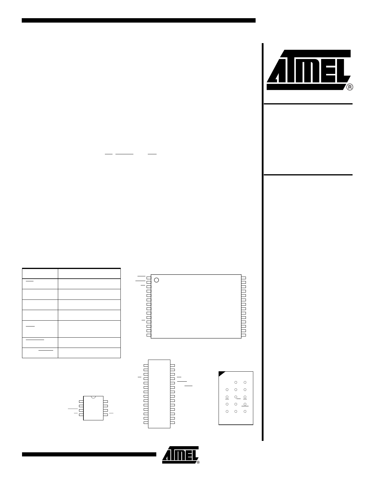
Pin Configurations
Pin Name Function
CS Chip Select
SCK
Serial Clock
SI Serial Input
SO Serial Output
WP
RESET
Hardware Page Write
Protect Pin
Chip Reset
RDY/BUSY Ready/Busy
8-SOIC
SI
SCK
RESET
CS
1
2
3
4
8 SO
7 GND
6 VCC
5 WP
RDY/BUSY
RESET
WP
NC
NC
VCC
GND
NC
NC
NC
CS
SCK
SI
SO
1
2
3
4
5
6
7
8
9
10
11
12
13
14
TSOP Top View
Type 1
28 NC
27 NC
26 NC
25 NC
24 NC
23 NC
22 NC
21 NC
20 NC
19 NC
18 NC
17 NC
16 NC
15 NC
28-SOIC
GND
NC
NC
CS
SCK
SI
SO
NC
NC
NC
NC
NC
NC
NC
1
2
3
4
5
6
7
8
9
10
11
12
13
14
28 VCC
27 NC
26 NC
25 WP
24 RESET
23 RDY/BUSY
22 NC
21 NC
20 NC
19 NC
18 NC
17 NC
16 NC
15 NC
CBGA Top View
through Package
12 3
A
NC NC
B
SCK GND VCC
C
CS RDY/BSY WP
D
SO SI RESET
E
NC NC NC
Rev. 1938F–DFLSH–10/02
1
1 page 
Program and Erase
Commands
1938F–DFLSH–10/02
AT45DB041B
loaded into the device. After the last bit of the opcode is shifted in, the eight bits of the
status register, starting with the MSB (bit 7), will be shifted out on the SO pin during the
next eight clock cycles. The five most significant bits of the status register will contain
device information, while the remaining three least-significant bits are reserved for future
use and will have undefined values. After bit 0 of the status register has been shifted
out, the sequence will repeat itself (as long as CS remains low and SCK is being tog-
gled) starting again with bit 7. The data in the status register is constantly updated, so
each repeating sequence will output new data.
Status Register Format
Bit 7
RDY/BUSY
Bit 6
COMP
Bit 5
0
Bit 4
1
Bit 3
1
Bit 2
1
Bit 1
X
Bit 0
X
Ready/Busy status is indicated using bit 7 of the status register. If bit 7 is a 1, then the
device is not busy and is ready to accept the next command. If bit 7 is a 0, then the
device is in a busy state. The user can continuously poll bit 7 of the status register by
stopping SCK at a low level once bit 7 has been output. The status of bit 7 will continue
to be output on the SO pin, and once the device is no longer busy, the state of SO will
change from 0 to 1. There are eight operations which can cause the device to be in a
busy state: Main Memory Page to Buffer Transfer, Main Memory Page to Buffer Com-
pare, Buffer to Main Memory Page Program with Built-in Erase, Buffer to Main Memory
Page Program without Built-in Erase, Page Erase, Block Erase, Main Memory Page
Program, and Auto Page Rewrite.
The result of the most recent Main Memory Page to Buffer Compare operation is indi-
cated using bit 6 of the status register. If bit 6 is a 0, then the data in the main memory
page matches the data in the buffer. If bit 6 is a 1, then at least one bit of the data in the
main memory page does not match the data in the buffer.
The device density is indicated using bits 5, 4, 3 and 2 of the status register. For the
AT45DB041B, the four bits are 0, 1, 1 and 1. The decimal value of these four binary bits
does not equate to the device density; the four bits represent a combinational code
relating to differing densities of Serial DataFlash devices, allowing a total of sixteen dif-
ferent density configurations.
BUFFER WRITE: Data can be shifted in from the SI pin into either buffer 1 or buffer 2.
To load data into either buffer, an 8-bit opcode, 84H for buffer 1 or 87H for buffer 2, must
be followed by 15 don’t care bits and nine address bits (BFA8 - BFA0). The nine
address bits specify the first byte in the buffer to be written. The data is entered following
the address bits. If the end of the data buffer is reached, the device will wrap around
back to the beginning of the buffer. Data will continue to be loaded into the buffer until a
low-to-high transition is detected on the CS pin.
BUFFER TO MAIN MEMORY PAGE PROGRAM WITH BUILT-IN ERASE: Data written
into either buffer 1 or buffer 2 can be programmed into the main memory. To start the
operation, an 8-bit opcode, 83H for buffer 1 or 86H for buffer 2, must be followed by the
four reserved bits, 11 address bits (PA10 - PA0) that specify the page in the main
memory to be written, and nine additional don’t care bits. When a low-to-high transition
occurs on the CS pin, the part will first erase the selected page in main memory to all 1s
and then program the data stored in the buffer into the specified page in the main mem-
ory. Both the erase and the programming of the page are internally self-timed and
should take place in a maximum time of tEP. During this time, the status register will indi-
cate that the part is busy.
5
5 Page 
AT45DB041B
Table 4. Detailed Bit-level Addressing Sequence
Address Byte
Address Byte
Address Byte
Opcode
Opcode
Additional
Don’t Care
Bytes
Required
50H 0 1 0 1 0 0 0 0 r r r r P P P P P P P P x x x x x x x x x x x x
N/A
52H 0 1 0 1 0 0 1 0 r r r r P P P P P P P P P P P B B B B B B B B B 4 Bytes
53H 0 1 0 1 0 0 1 1 r r r r P P P P P P P P P P P x x x x x x x x x
N/A
54H 0 1 0 1 0 1 0 0 x x x x x x x x x x x x x x x B B B B B B B B B
1 Byte
55H 0 1 0 1 0 1 0 1 r r r r P P P P P P P P P P P x x x x x x x x x
N/A
56H 0 1 0 1 0 1 1 0 x x x x x x x x x x x x x x x B B B B B B B B B
1 Byte
57H 0 1 0 1 0 1 1 1
N/A
N/A
N/A N/A
58H 0 1 0 1 1 0 0 0 r r r r P P P P P P P P P P P x x x x x x x x x
N/A
59H 0 1 0 1 1 0 0 1 r r r r P P P P P P P P P P P x x x x x x x x x
N/A
60H 0 1 1 0 0 0 0 0 r r r r P P P P P P P P P P P x x x x x x x x x
N/A
61H 0 1 1 0 0 0 0 1 r r r r P P P P P P P P P P P x x x x x x x x x
N/A
68H 0 1 1 0 1 0 0 0 r r r r P P P P P P P P P P P B B B B B B B B B 4 Bytes
81H 1 0 0 0 0 0 0 1 r r r r P P P P P P P P P P P x x x x x x x x x
N/A
82H 1 0 0 0 0 0 1 0 r r r r P P P P P P P P P P P B B B B B B B B B
N/A
83H 1 0 0 0 0 0 1 1 r r r r P P P P P P P P P P P x x x x x x x x x
N/A
84H 1 0 0 0 0 1 0 0 x x x x x x x x x x x x x x x B B B B B B B B B
N/A
85H 1 0 0 0 0 1 0 1 r r r r P P P P P P P P P P P B B B B B B B B B
N/A
86H 1 0 0 0 0 1 1 0 r r r r P P P P P P P P P P P x x x x x x x x x
N/A
87H 1 0 0 0 0 1 1 1 x x x x x x x x x x x x x x x B B B B B B B B B
N/A
88H 1 0 0 0 1 0 0 0 r r r r P P P P P P P P P P P x x x x x x x x x
N/A
89H 1 0 0 0 1 0 0 1 r r r r P P P P P P P P P P P x x x x x x x x x
N/A
D2H 1 1 0 1 0 0 1 0 r r r r P P P P P P P P P P P B B B B B B B B B 4 Bytes
D4H 1 1 0 1 0 1 0 0 x x x x x x x x x x x x x x x B B B B B B B B B
1 Byte
D6H 1 1 0 1 0 1 1 0 x x x x x x x x x x x x x x x B B B B B B B B B
1 Byte
D7H 1 1 0 1 0 1 1 1
N/A
N/A
N/A N/A
E8H 1 1 1 0 1 0 0 0 r r r r P P P P P P P P P P P B B B B B B B B B
Note:
r = Reserved Bit
P = Page Address Bit
B = Byte/Buffer Address Bit
x = Don’t Care
4 Bytes
1938F–DFLSH–10/02
11
11 Page | ||
| Páginas | Total 33 Páginas | |
| PDF Descargar | [ Datasheet AT45DB041B.PDF ] | |
Hoja de datos destacado
| Número de pieza | Descripción | Fabricantes |
| AT45DB041 | 4-Megabit 2.7-volt Only Serial DataFlash | ATMEL Corporation |
| AT45DB041-CC | 4-Megabit 2.7-volt Only Serial DataFlash | ATMEL Corporation |
| AT45DB041-CI | 4-Megabit 2.7-volt Only Serial DataFlash | ATMEL Corporation |
| AT45DB041-JC | 4-Megabit 2.7-volt Only Serial DataFlash | ATMEL Corporation |
| Número de pieza | Descripción | Fabricantes |
| SLA6805M | High Voltage 3 phase Motor Driver IC. |
Sanken |
| SDC1742 | 12- and 14-Bit Hybrid Synchro / Resolver-to-Digital Converters. |
Analog Devices |
|
DataSheet.es es una pagina web que funciona como un repositorio de manuales o hoja de datos de muchos de los productos más populares, |
| DataSheet.es | 2020 | Privacy Policy | Contacto | Buscar |