|
|
|
PDF AT49HLV010-55TI Data sheet ( Hoja de datos )
| Número de pieza | AT49HLV010-55TI | |
| Descripción | 1-Megabit 128K x 8 Single 2.7-volt Battery-Voltage Flash Memory | |
| Fabricantes | ATMEL Corporation | |
| Logotipo | ||
Hay una vista previa y un enlace de descarga de AT49HLV010-55TI (archivo pdf) en la parte inferior de esta página. Total 11 Páginas | ||
|
No Preview Available !
AT49(H)BV/(H)LV01
Features
• Single Supply Voltage, Range 2.7V to 3.6V
• Single Supply for Read and Write
• Fast Read Access Time - 55 ns
• Internal Program Control and Timer
• 8K bytes Boot Block With Lockout
• Fast Erase Cycle Time - 10 seconds
• Byte By Byte Programming - 30 µs/Byte typical
• Hardware Data Protection
• DATA Polling For End Of Program Detection
• Low Power Dissipation
– 25 mA Active Current
– 50 µA CMOS Standby Current
• Typical 10,000 Write Cycles
Description
The AT49(H)BV010 and the AT49(H)LV010 are 3-volt-only, 1-megabit Flash memo-
ries organized as 131,072 words of 8 bits each. Manufactured with Atmel’s advanced
nonvolatile CMOS technology, the devices offer access times to 55 ns with power dis-
sipation of just 90 mW over the commercial temperature range. When the devices are
deselected, the CMOS standby current is less than 50 µA.
To allow for simple in-system reprogrammability, the AT49(H)BV/(H)LV010 does not
require high input voltages for programming. Three-volt-only commands determine
the read and programming operation of the device. Reading data out of the device is
similar to reading from an EPROM. Reprogramming the AT49(H)BV/(H)LV010 is
performed by erasing the entire 1 megabit of memory and then programming on a
byte by byte basis. The typical byte programming time is a fast 30 µs. The end of a
program cycle can be optionally detected by the DATA polling feature. Once the end
of a byte program cycle has been detected, a new access for a read or program can
begin. The typical number of program and erase cycles is in excess of 10,000 cycles.
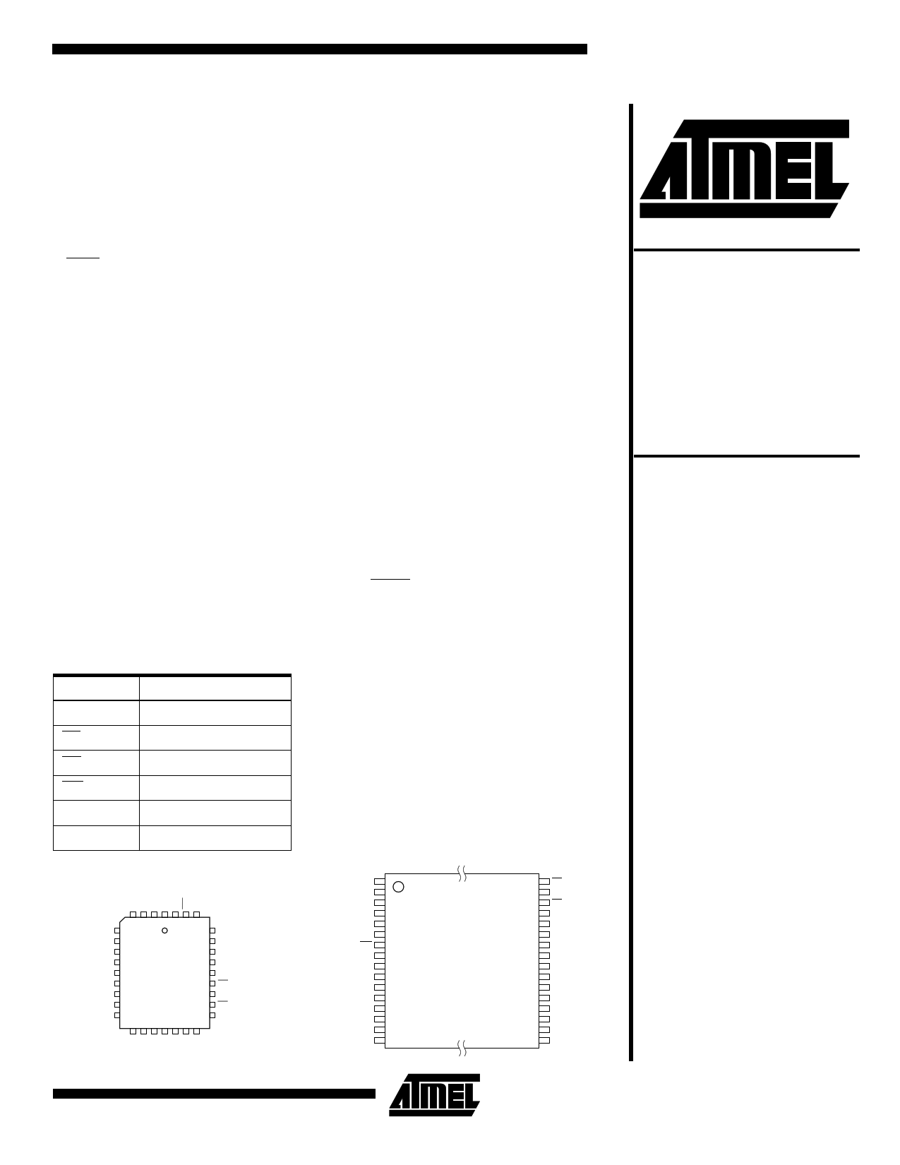
Pin Configurations
(continued)
Pin Name
A0 - A16
CE
OE
WE
I/O0 - I/O7
NC
Function
Addresses
Chip Enable
Output Enable
Write Enable
Data Inputs/Outputs
No Connect
TSOP Top View
Type 1
PLCC Top View
A7 5
A6 6
A5 7
A4 8
A3 9
A2 10
A1 11
A0 12
I/O0 13
29 A14
28 A13
27 A8
26 A9
25 A11
24 OE
23 A10
22 CE
21 I/O7
A11
A9
A8
A13
A14
NC
WE
VCC
NC
A16
A15
A12
A7
A6
A5
A4
1
2
3
4
5
6
7
8
9
10
11
12
13
14
15
16
32 OE
31 A10
30 CE
29 I/O7
28 I/O6
27 I/O5
26 I/O4
25 I/O3
24 GND
23 I/O2
22 I/O1
21 I/O0
20 A0
19 A1
18 A2
17 A3
1-Megabit
(128K x 8)
Single 2.7-volt
Battery-Voltage™
Flash Memory
AT49BV010
AT49HBV010
AT49LV010
AT49HLV010
0677B-A–9/97
1
1 page 
AT49(H)BV/(H)LV010
AC Read Characteristics
Symbol
tACC
tCE (1)
tOE (2)
tDF (3, 4)
tOH
Parameter
Address to Output Delay
CE to Output Delay
OE to Output Delay
CE or OE to Output
Float
Output Hold from OE,
CE or Address,
whichever occurred first
AT49HLV
010-55
Min Max
55
55
30
0 25
0
AC Read Waveforms(1)(2)(3)(4)
ADDRESS
AT49HBV/
HLV010-70
Min Max
70
70
35
0 25
AT49HBV/
HLV010-90
Min Max
90
90
40
0 25
00
ADDRESS VALID
AT49BV/
LV010-12
Min Max
120
120
50
0 30
AT49BV010-
15
Min Max
150
150
0 70
0 40
00
Units
ns
ns
ns
ns
ns
CE
tCE
OE
OUTPUT
tACC
HIGH Z
tOH
OUTPUT VALID
tDF
Notes:
1. CE may be delayed up to tACC - tCE after the address transition without impact on tACC.
2. OE may be delayed up to tCE - tOE after the falling edge of CE without impact on tCE or by tACC - tOE after an address change
without impace on tACC.
3. tDF is specified from OE or CE whichever occurs frist (CL - 5 pF).
4. This parameter is characterized and is not 100% tested.
Input Test Waveforms and
Measurement Level
AC 2.4V
DRIVING
LEVELS 0.4V
tR, tF < 5 ns
1.5V
AC
MEASUREMENT
LEVEL
Output Test Load
55/70 ns
3.0V
90/120/150 ns
3.0V
1.8K
1.3K
OUTPUT
PIN
30 pF
1.8K
1.3K
OUTPUT
PIN
100 pF
Pin Capacitance (f = 1 MHz, T = 25°C)(1)
Typ Max
CIN
COUT
Note:
46
8 12
1. This parameter is characterized and is not 100% tested.
Units
pF
pF
Conditions
VIN = 0V
VOUT = 0V
5
5 Page 
Ordering Information (Continued)
tACC
ICC (mA)
(ns) Active Standby Ordering Code
55 25
0.05 AT49HLV010-55JC
AT49HLV010-55TC
25 0.05 AT49HLV010-55JI
AT49HLV010-55TI
70 25
0.05 AT49HLV010-70JC
AT49HLV010-70TC
25 0.05 AT49HLV010-70JI
AT49HLV010-70TI
90 25
0.05 AT49HLV010-90JC
AT49HLV010-90TC
25 0.05 AT49HLV010-90JI
AT49HLV010-90TI
120 25
0.05 AT49LV010-12JC
AT49LV010-12TC
25 0.05 AT49LV010-12JI
AT49LV010-12TI
AT49(H)BV/(H)LV010
Package
32J
32T
32J
32T
32J
32T
32J
32T
32J
32T
32J
32T
32J
32T
32J
32T
Operation Range
Commercial
(0°C - 70°C)
Industrial
(-40°C - 85°C)
Commercial
(0°C - 70°C)
Industrial
(-40°C - 85°C)
Commercial
(0°C - 70°C)
Industrial
(-40°C - 85°C)
Commercial
(0°C - 70°C)
Industrial
(-40°C - 85°C)
Package Type
32J 32-Lead, Plastic J-Leaded Chip Carrier Package (PLCC)
32T 32-Lead, Thin Small Outline Package (TSOP)
11
11 Page | ||
| Páginas | Total 11 Páginas | |
| PDF Descargar | [ Datasheet AT49HLV010-55TI.PDF ] | |
Hoja de datos destacado
| Número de pieza | Descripción | Fabricantes |
| AT49HLV010-55TC | 1-Megabit 128K x 8 Single 2.7-volt Battery-Voltage Flash Memory | ATMEL Corporation |
| AT49HLV010-55TI | 1-Megabit 128K x 8 Single 2.7-volt Battery-Voltage Flash Memory | ATMEL Corporation |
| Número de pieza | Descripción | Fabricantes |
| SLA6805M | High Voltage 3 phase Motor Driver IC. |
Sanken |
| SDC1742 | 12- and 14-Bit Hybrid Synchro / Resolver-to-Digital Converters. |
Analog Devices |
|
DataSheet.es es una pagina web que funciona como un repositorio de manuales o hoja de datos de muchos de los productos más populares, |
| DataSheet.es | 2020 | Privacy Policy | Contacto | Buscar |