|
|
|
PDF ADXL05 Data sheet ( Hoja de datos )
| Número de pieza | ADXL05 | |
| Descripción | +-1 g to +-5 g Single Chip Accelerometer with Signal Conditioning | |
| Fabricantes | Analog Devices | |
| Logotipo | ||
Hay una vista previa y un enlace de descarga de ADXL05 (archivo pdf) en la parte inferior de esta página. Total 20 Páginas | ||
|
No Preview Available !
a ؎1 g to ؎5 g Single Chip Accelerometer
with Signal Conditioning
ADXL05*
FEATURES
5 milli-g Resolution
Noise Level 12؋ Less than the ADXL50
User Selectable Full Scale from ؎1 g to ؎5 g
Output Scale Selectable from 200 mV/g to 1 V/g
Complete Acceleration Measurement System on a
Single Chip IC
Self Test on Digital Command
+5 V Single Supply Operation
1000 g Shock Survival
APPLICATIONS
Low Cost Sensor for Vibration Measurement
Tilt Sensing with Faster Response than Electrolytic or
Mercury Sensors
More Sensitive Alarms and Motion Detectors
Affordable Inertial Sensing of Velocity and Position
GENERAL DESCRIPTION
The ADXL05 is a complete acceleration measurement system
on a single monolithic IC. The ADXL05 will measure accelera-
tions with full-scale ranges of ± 5 g to ± 1 g or less. Typical noise
floor is 500 µg/√Hz, (12× less than the ADXL50), allowing sig-
nals below 5 milli-g to be resolved. The ADXL05 is a force bal-
anced capacitive accelerometer with the capability to measure
both ac accelerations (typical of vibration) or dc accelerations
(such as inertial force or gravity). Three external capacitors and
a +5 volt regulated power supply are all that is required to
measure accelerations up to ± 5 g. Three resistors are used to
configure the output buffer amplifier to set scale factors from
200 mV/g to 1 V/g. External capacitors may be added to the
resistor network to provide 1 or 2 poles of filtering. No addi-
tional active components are required to interface directly to
most analog to digital converters (ADCs).
The device features a TTL compatible self-test function that
can electrostatically deflect the sensor beam at any time to verify
that the sensor and its electronics are functioning correctly.
The ADXL05 is available in a hermetic 10-pin TO-100 metal
can, specified over the 0°C to +70°C commercial, and –40°C to
+85°C industrial temperature ranges. Contact factory for avail-
ability of automotive grade devices.
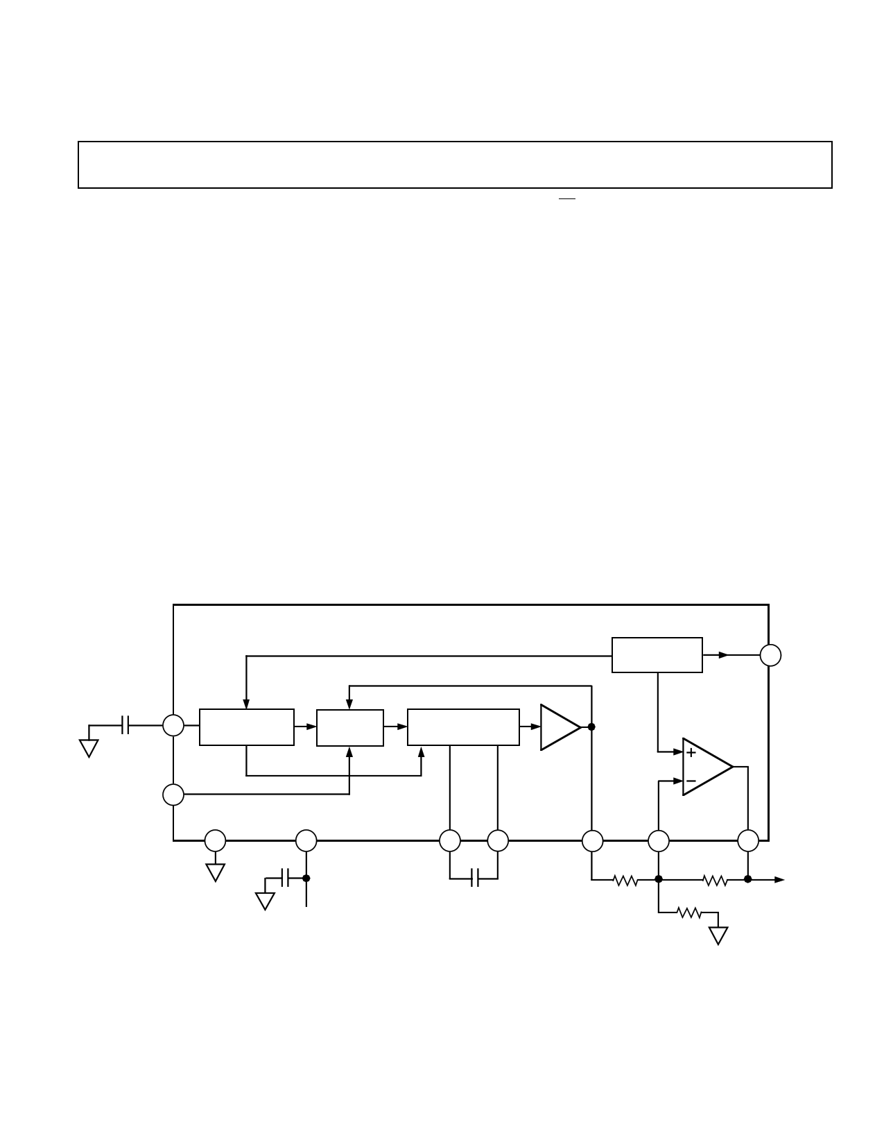
FUNCTIONAL BLOCK DIAGRAM
ADXL05
OSCILLATOR
DECOUPLING
CAPACITOR
4
C2
OSCILLATOR
SENSOR
SELF-TEST
(ST)
7
5
COM
1
C3
+5V
DEMODULATOR
PREAMP
REFERENCE
+3.4V
6 VREF
OUTPUT
+1.8V
2
C1
3
C1
DEMODULATOR
CAPACITOR
8
VPR
BUFFER
AMP
10
R1 VIN– R3
9
R2
VOUT
*Patents pending.
REV. B
Information furnished by Analog Devices is believed to be accurate and
reliable. However, no responsibility is assumed by Analog Devices for its
use, nor for any infringements of patents or other rights of third parties
which may result from its use. No license is granted by implication or
otherwise under any patent or patent rights of Analog Devices.
© Analog Devices, Inc., 1996
One Technology Way, P.O. Box 9106, Norwood. MA 02062-9106, U.S.A.
Tel: 617/329-4700
Fax: 617/326-8703
1 page 
ADXL05
GLOSSARY OF TERMS
Acceleration: Change in velocity per unit time.
Acceleration Vector: Vector describing the net acceleration
acting upon the ADXL05 (AXYZ).
g: A unit of acceleration equal to the average force of gravity
occurring at the earth’s surface. A g is approximately equal to
32.17 feet/s2, or 9.807 meters/s2.
Nonlinearity: The maximum deviation of the ADXL05 output
voltage from a best fit straight line fitted to a plot of acceleration
vs. output voltage, calculated as a % of the full-scale output
voltage (@ 5 g).
Resonant Frequency: The natural frequency of vibration of
the ADXL05 sensor’s central plate (or “beam”). At its resonant
frequency of 12 kHz, the ADXL05’s moving center plate has a
peak in its frequency response with a Q of 3 or 4.
Sensitivity: The output voltage change per g unit of accelera-
tion applied, specified at the VPR pin in mV/g.
Sensitive Axis (X): The most sensitive axis of the accelerom-
eter sensor. Defined by a line drawn between the package tab
and Pin 5 in the plane of the pin circle. See Figures 2a and 2b.
Sensor Alignment Error: Misalignment between the
ADXL05’s on-chip sensor and the package axis, defined by
Pin 5 and the package tab.
Total Alignment Error: Net misalignment of the ADXL05’s
on-chip sensor and the measurement axis of the application.
This error includes errors due to sensor die alignment to the
package, and any misalignment due to installation of the sensor
package in a circuit board or module.
Transverse Acceleration: Any acceleration applied 90° to the
axis of sensitivity.
Transverse Sensitivity Error: The percent of a transverse ac-
celeration that appears at the VPR output. For example, if the
transverse sensitivity is 1%, then a +10 g transverse acceleration
will cause a 0.1 g signal to appear at VPR (1% of 10 g). Trans-
verse sensitivity can result from a sensitivity of the sensor to
transverse forces or from misalignment of the internal sensor to
its package.
Transverse Y Axis: The axis perpendicular (90°) to the pack-
age axis of sensitivity in the plane of the package pin circle. See
Figure 2.
Transverse Z Axis: The axis perpendicular (90°) to both the
package axis of sensitivity and the plane of the package pin
circle. See Figure 2.
Polarity of the Acceleration Output
The polarity of the ADXL05 output is shown in the Figure 1.
When oriented to the earth’s gravity (and held in place), the
ADXL05 will experience an acceleration of +1 g. This corre-
sponds to a change of approximately +200 mV at the VPR out-
put pin. Note that the polarity will be reversed to a negative
going signal at the buffer amplifier output VOUT, due to its
inverting configuration.
TAB
+1g +
–
PIN 5
INDICATED POLARITY IS THAT
OCCURRING AT VPR .
Figure 1. Output Polarity at VPR
Acceleration Vectors in Three Dimensions
The ADXL05 is a sensor designed to measure accelerations that
result from an applied force. The ADXL05 responds to the
component of acceleration on its sensitive X axis. Figures 2a
and 2b show the relationship between the sensitive “X” axis and
the transverse “Z” and “Y” axes as they relate to the TO-100
SIDE VIEW
Z
TRANSVERSE Z AXIS
X
PIN 5
X
TAB SENSITIVE (X) AXIS
Z
Figure 2a. Sensitive X and Transverse Z Axis
TOP VIEW
Y
TRANSVERSE Y AXIS
X
PIN 5
X
TAB SENSITIVE (X) AXIS
Y
Figure 2b. Sensitive X and Transverse Y Axis
REV. B
–5–
5 Page 
ADXL05
USING THE INTERNAL BUFFER AMPLIFIER TO VARY
THE ACCELEROMETER’S OUTPUT SCALE FACTOR
AND 0 g BIAS LEVEL
The ADXL05 accelerometer has an onboard buffer amplifier
that allows the user to change the output scale factor and 0 g
bias level.
The output scale factor of an accelerometer is simply how many
volts output are provided per g of applied acceleration. This
should not be confused with its resolution. The resolution of the
device is the lowest g level the accelerometer is capable of mea-
suring. Resolution is principally determined by the device noise
and the measurement bandwidth.
The 0 g bias level is simply the dc output level of the accelerom-
eter when it is not in motion or being acted upon by the Earth’s
gravity.
Setting the Accelerometer’s Scale Factor
Figure 20 shows the basic connections for using the onboard
buffer amplifier to increase the output scale factor. The nominal
output level in volts from VPR (the preamplifier output) is equal
to the g forces applied to the sensor (along its sensitive axis)
times 200 mV/g. The use of the buffer is always recommended,
even if the preset scale factor is adequate, as the buffer helps
prevent any following circuitry from loading down the VPR
output.
C2
4
0.022µF
0.022µF
C1
2
3
C1
ADXL05
PRE-AMP
1
1.8V
BUFFER
AMP
9
5
COM
6
+3.4V
REF
8
VPR
R1
10
VIN–
R3
OUTPUT SCALE FACTOR =
VPR OUTPUT: 200mV/g
R3
R1
x
VPR
OUTPUT
+5V
C3
0.1µF
VOUT
Figure 20. Basic Buffer Connections
In Figure 20, the output scale factor at Pin 9 (VOUT) is the out-
put at VPR times the gain of the buffer, which is simply the value
of resistor R3 divided by R1. Choose a convenient scale factor,
keeping in mind that the buffer gain not only amplifies the sig-
nal but any noise or drift as well. Too much gain can also cause
the buffer to saturate and clip the output wave form.
The circuit of Figure 20 is entirely adequate for many applica-
tions, but its accuracy is dependent on the pretrimmed accuracy
of the accelerometer and this will vary by product type and
grade. For the highest possible accuracy, an external trim is rec-
ommended. As shown by Figure 21, this consists of a potenti-
ometer, R1a, in series with a fixed resistor, R1b.
C2
4
0.022µF
0.022µF
C1
2
3
C1
ADXL05
PRE-AMP
1
1.8V
BUFFER
AMP
9
COM
5
6
+3.4V
REF
8
VPR
10
VIN–
R1a R1b
R3
OUTPUT SCALE FACTOR =
VPR OUTPUT: 200mV/g
R3
(R1a + R1b)
x VPR OUTPUT
+5V
0.1µF
VOUT
Figure 21. External Scale Factor Trimming
Setting the Accelerometer’s 0 g Bias Level, AC Coupled
Response
If a dc (gravity) response is not required—for example in motion
sensing or vibration measurement applications—ac coupling can
be used between the preamplifier output and the buffer input as
shown in Figure 22. The use of ac coupling between VPR and
the buffer input virtually eliminates any 0 g drift and allows the
maximum buffer gain without clipping.
Resistor R1 and capacitor C4 together form a high pass filter
whose corner frequency is 1/(2 π R1 C4). This means that this
simple filter will reduce the signal from VPR by 3 dB at the
corner frequency, and it will continue to reduce it at a rate of
6 dB/octave (20 dB per decade) for signals below the corner
frequency.
Note that capacitor C4 should be a nonpolarized, low leakage
type. If a polarized capacitor is used, tantalum types are pre-
ferred, rather than electrolytic. With polarized capacitors, VPR
should be measured on each device and the positive terminal of
the capacitor connected toward either VPR or VIN—whichever is
more positive
The 0 g offset level of the ADXL05 accelerometer is preset at
+1.8 V. This can easily be changed to a more convenient level,
such as +2.5 V which, being at the middle of the supply voltage,
provides the greatest output voltage swing.
When using the ac coupled circuit of Figure 22, only a single re-
sistor, R2, is required to swing the buffer output to +2.5 V.
Since the “+” input of the buffer is referenced at +1.8 V, its
summing junction, Pin 10, is also held constant at +1.8 V.
Therefore, to swing the buffer’s output to the desired +2.5 V
0 g bias level, its output must move up +0.7 V (2.5 V – 1.8 V =
0.7 V). Therefore, the current needed to flow through R3 to
cause this change, IR3, is equal to:
IR 3
=
0.7 Volts
R3 in Ohms
REV. B
–11–
11 Page | ||
| Páginas | Total 20 Páginas | |
| PDF Descargar | [ Datasheet ADXL05.PDF ] | |
Hoja de datos destacado
| Número de pieza | Descripción | Fabricantes |
| ADXL001 | Wide Bandwidth Accelerometer | Analog Devices |
| ADXL05 | +-1 g to +-5 g Single Chip Accelerometer with Signal Conditioning | Analog Devices |
| Número de pieza | Descripción | Fabricantes |
| SLA6805M | High Voltage 3 phase Motor Driver IC. |
Sanken |
| SDC1742 | 12- and 14-Bit Hybrid Synchro / Resolver-to-Digital Converters. |
Analog Devices |
|
DataSheet.es es una pagina web que funciona como un repositorio de manuales o hoja de datos de muchos de los productos más populares, |
| DataSheet.es | 2020 | Privacy Policy | Contacto | Buscar |