|
|
|
PDF AD8304 Data sheet ( Hoja de datos )
| Número de pieza | AD8304 | |
| Descripción | 160 dB Range (100 pA -10 mA) Logarithmic Converter | |
| Fabricantes | Analog Devices | |
| Logotipo | ||
1. AD8304 Hay una vista previa y un enlace de descarga de AD8304 (archivo pdf) en la parte inferior de esta página. Total 20 Páginas | ||
|
No Preview Available !
a
FEATURES
Optimized for Fiber Optic Photodiode Interfacing
Eight Full Decades of Range
Law Conformance 0.1 dB from 1 nA to 1 mA
Single-Supply Operation (3.0 V– 5.5 V)
Complete and Temperature Stable
Accurate Laser-Trimmed Scaling:
Logarithmic Slope of 10 mV/dB (at VLOG Pin)
Basic Logarithmic Intercept at 100 pA
Easy Adjustment of Slope and Intercept
Output Bandwidth of 10 MHz, 15 V/s Slew Rate
1-, 2-, or 3-Pole Low-Pass Filtering at Output
Miniature 14-Lead Package (TSSOP)
Low Power: ~4.5 mA Quiescent Current (Enabled)
APPLICATIONS
High Accuracy Optical Power Measurement
Wide Range Baseband Log Compression
Versatile Detector for APC Loops
160 dB Range (100 pA –10 mA)
Logarithmic Converter
AD8304
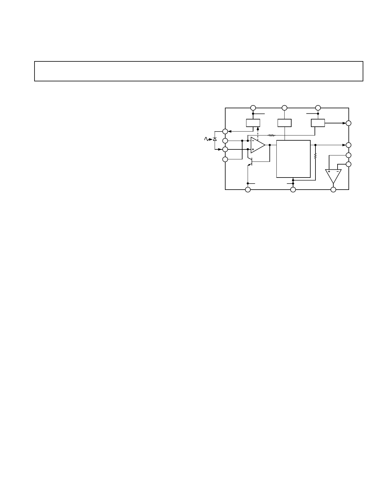
FUNCTIONAL BLOCK DIAGRAM
VPDB
6
VSUM
3
IPD INPT
4
VSUM 5
VPS2
10
PWDN
2
PDB
BIAS
~10k⍀
VPS1
12
AD8304
VREF
7 VREF
0.5V
TEMPERATURE
COMPENSATION
5k⍀
8 VLOG
9 BFIN
13 BFNG
1
VNEG
14
ACOM
11
VOUT
PRODUCT DESCRIPTION
The AD8304 is a monolithic logarithmic detector optimized for
the measurement of low frequency signal power in fiber optic
systems. It uses an advanced translinear technique to provide an
exceptionally large dynamic range in a versatile and easily used
form. Its wide measurement range and accuracy are achieved
using proprietary design techniques and precise laser trimming.
In most applications only a single positive supply, VP, of 5 V
will be required, but 3.0 V to 5.5 V can be used, and certain
applications benefit from the added use of a negative supply,
VN. When using low supply voltages, the log slope is readily
altered to fit the available span. The low quiescent current and
chip disable features facilitate use in battery-operated applications.
The input current, IPD, flows in the collector of an optimally
scaled NPN transistor, connected in a feedback path around a
low offset JFET amplifier. The current-summing input node
operates at a constant voltage, independent of current, with a
default value of 0.5 V; this may be adjusted over a wide range,
including ground or below, using an optional negative supply.
An adaptive biasing scheme is provided for reducing the dark
current at very low light input levels. The voltage at Pin VPDB
applies approximately 0.1 V across the diode for IPD = 100 pA,
rising linearly with current to 2.0 V of net bias at IPD = 10 mA.
The input pin INPT is flanked by the guard pins VSUM that
track the voltage at the summing node to minimize leakage.
The default value of the logarithmic slope at the output VLOG is
accurately scaled to 10 mV/dB (200 mV/decade). The resistance
at this output is laser-trimmed to 5 kΩ, allowing the slope to be
lowered by shunting it with an external resistance; the addition
of a capacitor at this pin provides a simple low-pass filter. The
intermediate voltage VLOG is buffered in an output stage that can
swing to within about 100 mV of ground (or VN) and the posi-
tive supply, VP, and provides a peak current drive capacity of
± 20 mA. The slope can be increased using the buffer and a pair
of external feedback resistors. An accurate voltage reference of
2 V is also provided to facilitate the repositioning of the intercept.
Many operational modes are possible. For example, low-pass filters
of up to three poles may be implemented, to reduce the output
noise at low input currents. The buffer may also serve as a com-
parator, with or without hysteresis, using the 2 V reference, for
example, in alarm applications. The incremental bandwidth of
a translinear logarithmic amplifier inherently diminishes for small
input currents. At the 1 nA level, the AD8304’s bandwidth is
about 2 kHz, but this increases in proportion to IPD up to a
maximum value of 10 MHz.
The AD8304 is available in a 14-lead TSSOP package and specified
for operation from –40°C to +85°C.
REV. A
Information furnished by Analog Devices is believed to be accurate and
reliable. However, no responsibility is assumed by Analog Devices for its
use, nor for any infringements of patents or other rights of third parties that
may result from its use. No license is granted by implication or otherwise
under any patent or patent rights of Analog Devices.
One Technology Way, P.O. Box 9106, Norwood, MA 02062-9106, U.S.A.
Tel: 781/329-4700
www.analog.com
Fax: 781/326-8703
© Analog Devices, Inc., 2002
1 page 
10
10nA100nA1A 10A
0 100A
1nA 10mA
–10 1mA
–20
–30
–40
–50
–60
–70
100
1k
10k 100k 1M
10M
100M
FREQUENCY – Hz
TPC 7. Small Signal AC Response, IPD to VLOG
(5% Sine Modulation of IPD at Frequency)
AD8304
10
9
8
7
6
5
4
3
2
1
0
1n
10n 100n 1
10 100 1m
10m
INPUT CURRENT – A
TPC 10. Total Wideband Noise Voltage at VLOG vs. IPD
100
10kHz
10
100kHz
1
1kHz
0.1 1MHz
100Hz
0.01
1n
10n 100n
1 10
IPD – A
100
1m
10m
TPC 8. Spot Noise Spectral Density at VLOG vs. IPD
3
GAIN = 1؋, 2؋, 2.5؋, 5؋
0
AV = 5
–3
AV = 2.5
–6
AV = 2
–9
AV = 1
–12
100
1k
10k 100k
1M
10M
100M
FREQUENCY – Hz
TPC 11. Small Signal Response of Buffer
100
1nA
10
10nA
100nA
1
0.1
1A
10A
>100A
0.01
100
1k 10k 100k 1M
FREQUENCY – Hz
10M
TPC 9. Spot Noise Spectral Density at VLOG vs. Frequency
10
fC = 1kHz
0
–10
–20
–30
–40
–50
–60
–70
10
100 1k 10k
FREQUENCY – Hz
100k
TPC 12. Small Signal Response of Buffer
Operating as Two-Pole Filter
REV. A
–5–
5 Page 
AD8304
In addition to uses in filter and comparator functions, the buffer
amplifier provides the means to adjust both the slope and inter-
cept, which require a minimal number of external components.
The high input impedance at BFIN, low input offset voltage,
large output swing, and wide bandwidth of this amplifier permit
numerous transformations of the basic VLOG signal, using stan-
dard op amp circuit practices. For example, it has been noted
that to raise the gain of the buffer, and therefore the slope, a
feedback attenuator, RA and RB in Figure 3, should be inserted
between VLOG and the inverting input Pin BFNG.
A wide range of gains may be used and the resistor magnitudes
are not critical; their parallel sum should be about equal to the
net source resistance at the noninverting input. When high gains
are used, the output dynamic range will be reduced; for maxi-
mum swing of 4.8 V, it will amount to simply 4.8 V/VY decades.
Thus, using a ratio of 3ϫ, to set up a slope 30 mV/dB (600 mV/
decade), eight decades can be handled, while with a ratio of 5ϫ,
which sets up a slope of 50 mV/dB (1 V/decade), the dynamic
range is 4.8 decades, or 96 dB. When using a lower positive
supply voltage, the calculation proceeds in the same way,
remembering to first subtract 0.2 V to allow for 0.1 V upper and
lower headroom in the output swing.
Alteration of the logarithmic intercept is only slightly more tricky.
First note that it will rarely be necessary to lower the intercept
below a value of 100 pA, since this merely raises all output volt-
ages further above ground. However, where this is required, the
first step is to raise the voltage VLOG by connecting a resistor, RZ,
from VLOG to VREF (2 V) as shown in Figure 4.
VPS2
10
IPD
VPDB
NC 6
VSUM
3
INPT
4
PDB
C1
VSUM
5
1nF
10nF
R1
750⍀
PWDN
2
VPS1
12
VP
BIAS
VREF
VREF
7
~10k⍀
0.5V
RZ
TEMPERATURE
COMPENSATION
5k⍀
VLOG
8
BFIN
9
BFNG
13
RA RB
1
VNEG
NC = NO CONNECT
14
ACOM
11
VOUT
VOUT
Figure 4. Method for Lowering the Intercept
This has the effect of elevating VLOG for small inputs while lower-
ing the slope to some extent because of the shunt effect of RZ
on the 5 kΩ output resistance. Then, if necessary, the slope may
be increased as before, using a feedback attenuator around the
buffer. Table II lists some examples of lowering the intercept
combined with various slope variations.
Table II. Examples of Lowering the Intercept
VY (mV/decade)
200
200
200
300
300
300
400
400
400
500
500
500
IZ (pA)
1
10
50
1
10
50
1
10
50
1
10
50
RA (k⍀)
20.0
10.0
3.01
10.0
8.06
6.65
11.5
9.76
8.66
16.5
14.3
13.0
RB (k⍀)
100
100
100
12.4
12.4
12.4
8.2
8.2
8.2
8.2
8.2
8.2
RZ (k⍀)
25
50
165
25
50
165
25
50
165
25
50
165
Equations for use with Table II:
VOUT
= GVY
×
RZ
RZ
+ RLOG
×
log10
I PD
IZ
+ VREF
×
RLOG
RLOG + RZ
where
G = 1 + RA
RB
and RLOG = 5 kΩ
Generally, it will be useful to raise the intercept. Keep in mind
that this moves the VLOG line in Figure 2 to the right, lowering all
output values. Figure 5 shows how this is achieved. The feedback
resistors, RA and RB, around the buffer are now augmented with
a third resistor, RZ, placed between the Pins BFNG and VREF.
This raises the zero-signal voltage on BFNG, which has the effect
of pushing VOUT lower. Note that the addition of this resistor also
alters the feedback ratio. However, this is readily compensated
in the design of the network. Table III lists the resistor values
for representative intercepts.
Table III. Examples of Raising the Intercept
VY (mV/decade)
300
300
400
400
400
500
500
500
IZ (nA)
10
100
10
100
500
10
100
500
RA (k⍀)
7.5
8.25
10
9.76
9.76
12.4
12.4
11.5
RB (k⍀)
37.4
130
16.5
25.5
36.5
12.4
16.5
20.0
RC(k⍀)
24.9
18.2
25.5
16.2
13.3
24.9
16.5
12.4
Equations for use with Table III:
VOUT
=G
VY
×
log10
IPD
IZ
– VREF
×
RA RB
RA RB + RC
where
G = 1 + RA
RB RC
and RA
RB
=
RA
RA
× RB
+ RB
REV. A
–11–
11 Page | ||
| Páginas | Total 20 Páginas | |
| PDF Descargar | [ Datasheet AD8304.PDF ] | |
Hoja de datos destacado
| Número de pieza | Descripción | Fabricantes |
| AD830 | High Speed Video Difference Amplifier | Analog Devices |
| AD8300 | +3 Volt/ Serial Input Complete 12-Bit DAC | Analog Devices |
| AD8302 | RF/IF Gain and Phase Detector | Analog Devices |
| AD8303 | +3 V/ Dual/ Serial Input Complete 12-Bit DAC | Analog Devices |
| Número de pieza | Descripción | Fabricantes |
| SLA6805M | High Voltage 3 phase Motor Driver IC. |
Sanken |
| SDC1742 | 12- and 14-Bit Hybrid Synchro / Resolver-to-Digital Converters. |
Analog Devices |
|
DataSheet.es es una pagina web que funciona como un repositorio de manuales o hoja de datos de muchos de los productos más populares, |
| DataSheet.es | 2020 | Privacy Policy | Contacto | Buscar |