|
|
|
PDF AD9281 Data sheet ( Hoja de datos )
| Número de pieza | AD9281 | |
| Descripción | Dual Channel 8-Bit Resolution CMOS ADC | |
| Fabricantes | Analog Devices | |
| Logotipo | ||
Hay una vista previa y un enlace de descarga de AD9281 (archivo pdf) en la parte inferior de esta página. Total 16 Páginas | ||
|
No Preview Available !
a
FEATURES
Complete Dual Matching ADC
Low Power Dissipation: 225 mW (+3 V Supply)
Single Supply: 2.7 V to 5.5 V
Differential Nonlinearity Error: 0.1 LSB
On-Chip Analog Input Buffers
On-Chip Reference
Signal-to-Noise Ratio: 49.2 dB
Over Seven Effective Bits
Spurious-Free Dynamic Range: –65 dB
No Missing Codes Guaranteed
28-Lead SSOP
Dual Channel 8-Bit
Resolution CMOS ADC
AD9281
IINA
IINB
IREFB
IREFT
QREFB
QREFT
VREF
REFSENSE
QINB
QINA
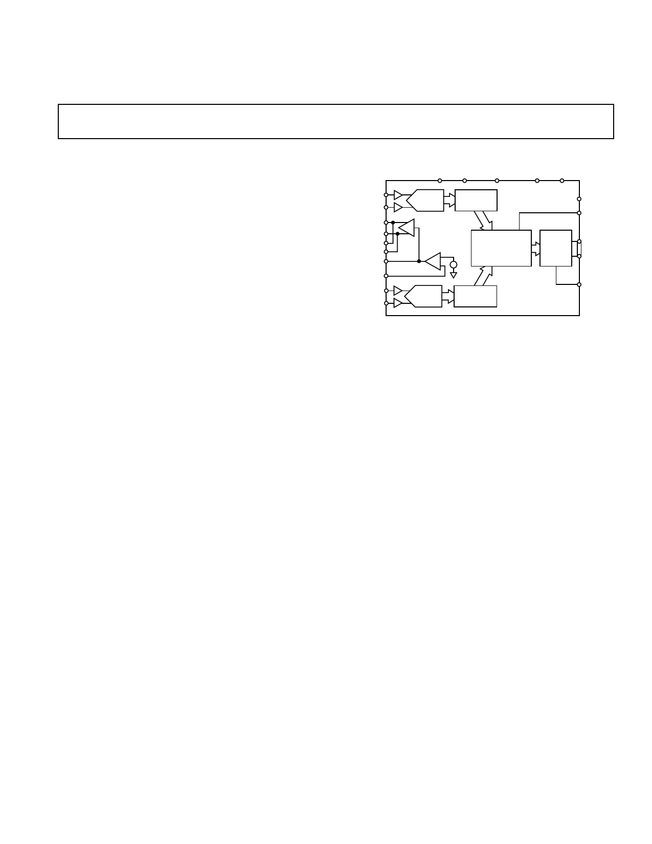
FUNCTIONAL BLOCK DIAGRAM
AVDD AVSS CLOCK
DVDD DVSS
"I" ADC
I
REGISTER
AD9281
REFERENCE
BUFFER
ASYNCHRONOUS
MULTIPLEXER
1V
THREE-
STATE
OUTPUT
BUFFER
"Q" ADC
Q
REGISTER
SLEEP
SELECT
DATA
8 BITS
CHIP
SELECT
PRODUCT DESCRIPTION
The AD9281 is a complete dual channel, 28 MSPS, 8-bit
CMOS ADC. The AD9281 is optimized specifically for applica-
tions where close matching between two ADCs is required (e.g.,
I/Q channels in communications applications). The 28 MHz
sampling rate and wide input bandwidth will cover both narrow-
band and spread-spectrum channels. The AD9281 integrates
two 8-bit, 28 MSPS ADCs, two input buffer amplifiers, an internal
voltage reference and multiplexed digital output buffers.
Each ADC incorporates a simultaneous sampling sample-and-
hold amplifier at its input. The analog inputs are buffered; no
external input buffer op amp will be required in most applica-
tions. The ADCs are implemented using a multistage pipeline
architecture that offers accurate performance and guarantees no
missing codes. The outputs of the ADCs are ported to a multi-
plexed digital output buffer.
The AD9281 is manufactured on an advanced low cost CMOS
process, operates from a single supply from 2.7 V to 5.5 V, and
consumes 225 mW of power (on 3 V supply). The AD9281
input structure accepts either single-ended or differential signals,
providing excellent dynamic performance up to and beyond
14 MHz Nyquist input frequencies.
PRODUCT HIGHLIGHTS
1. Dual 8-Bit, 28 MSPS ADC
A pair of high performance 28 MSPS ADCs that are opti-
mized for spurious free dynamic performance are provided for
encoding of I and Q or diversity channel information.
2. Low Power
Complete CMOS Dual ADC function consumes a low
225 mW on a single supply (on 3 V supply). The AD9281
operates on supply voltages from 2.7 V to 5.5 V.
3. On-Chip Voltage Reference
The AD9281 includes an on-chip compensated bandgap
voltage reference pin programmable for 1 V or 2 V.
4. On-chip analog input buffers eliminate the need for external
op amps in most applications.
5. Single 8-Bit Digital Output Bus
The AD9281 ADC outputs are interleaved onto a single
output bus saving board space and digital pin count.
6. Small Package
The AD9281 offers the complete integrated function in a
compact 28-lead SSOP package.
7. Product Family
The AD9281 dual ADC is pin compatible with a dual 10-bit
ADC (AD9201).
REV. F
Information furnished by Analog Devices is believed to be accurate and
reliable. However, no responsibility is assumed by Analog Devices for its
use, nor for any infringements of patents or other rights of third parties
which may result from its use. No license is granted by implication or
otherwise under any patent or patent rights of Analog Devices.
One Technology Way, P.O. Box 9106, Norwood, MA 02062-9106, U.S.A.
Tel: 781/329-4700 World Wide Web Site: http://www.analog.com
Fax: 781/461-3113 ©1999-2011 Analog Devices, Inc. All rights reserved.
1 page 
AD9281
ABSOLUTE MAXIMUM RATINGS*
Parameter
With
Respect
to Min
Max
Units
AVDD
AVSS
DVDD
DVSS
AVSS
DVSS
AVDD
DVDD
CLK
AVSS
Digital Outputs DVSS
AINA, AINB
AVSS
VREF
AVSS
REFSENSE
AVSS
REFT, REFB
AVSS
Junction Temperature
Storage Temperature
Lead Temperature
10 sec
–0.3
–0.3
–0.3
–6.5
–0.3
–0.3
–1.0
–0.3
–0.3
–0.3
–65
+6.5
+6.5
+0.3
+6.5
AVDD + 0.3
DVDD + 0.3
AVDD + 0.3
AVDD + 0.3
AVDD + 0.3
AVDD + 0.3
+150
+150
V
V
V
V
V
V
V
V
V
V
°C
°C
+300
°C
*Stresses above those listed under Absolute Maximum Ratings may cause perma-
nent damage to the device. This is a stress rating only; functional operation of the
device at these or any other conditions above those indicated in the operational
sections of this specification is not implied. Exposure to absolute maximum ratings
for extended periods may effect device reliability.
PIN CONFIGURATION
DVSS
DVDD
DNC
DNC
(LSB) D0
D1
D2
D3
D4
D5
D6
(MSB) D7
SELECT
CLOCK
AD9281
TOP VIEW
(Not to Scale)
CHIP-SELECT
INA-Q
INB-Q
REFT-Q
REFB-Q
AVDD
VREF
REFSENSE
AVSS
REFB-I
REFT-I
INB-I
INA-I
SLEEP
NC = NO CONNECT
PIN FUNCTION DESCRIPTIONS
Pin
No. Name
Description
1 DVSS
Digital Ground
2 DVDD
Digital Supply
3 DNC
Do not connect
4 DNC
Do not connect
5 D0
Bit 0 (LSB)
6 D1
Bit 1
7 D2
Bit 2
8 D3
Bit 3
9 D4
Bit 4
10 D5
Bit 5
11 D6
Bit 6
12 D7
Bit 7 (MSB)
13 SELECT
Hi I Channel Out, Lo Q Channel Out
14 CLOCK
Clock
15 SLEEP
Hi Power Down, Lo Normal Operation
16 INA-I
I Channel, A Input
17 INB-I
I Channel, B Input
18 REFT-I
Top Reference Decoupling, I Channel
19 REFB-I
Bottom Reference Decoupling, I Channel
20 AVSS
Analog Ground
21 REFSENSE Reference Select
22 VREF
Internal Reference Output
23 AVDD
Analog Supply
24 REFB-Q
Bottom Reference Decoupling, Q Channel
25 REFT-Q
Top Reference Decoupling, Q Channel
26 INB-Q
Q Channel B Input
27 INA-Q
Q Channel A Input
28 CHIP-SELECT Hi-High Impedance, Lo-Normal Operation
DEFINITIONS OF SPECIFICATIONS
INTEGRAL NONLINEARITY (INL)
Integral nonlinearity refers to the deviation of each individual
code from a line drawn from “zero” through “full scale.” The
point used as “zero” occurs 1/2 LSB before the first code transi-
tion. “Full scale” is defined as a level 1 1/2 LSBs beyond the last
code transition. The deviation is measured from the center of
each particular code to the true straight line.
DIFFERENTIAL NONLINEARITY (DNL, NO MISSING
CODES)
An ideal ADC exhibits code transitions that are exactly 1 LSB
apart. DNL is the deviation from this ideal value. It is often
specified in terms of the resolution for which no missing codes
(NMC) are guaranteed.
CAUTION
ESD (electrostatic discharge) sensitive device. Electrostatic charges as high as 4000 V readily
accumulate on the human body and test equipment and can discharge without detection.
Although the AD9281 features proprietary ESD protection circuitry, permanent damage may
occur on devices subjected to high energy electrostatic discharges. Therefore, proper ESD
precautions are recommended to avoid performance degradation or loss of functionality.
–4–
WARNING!
ESD SENSITIVE DEVICE
REV. F
5 Page 
AD9281
REFERENCE AND REFERENCE BUFFER
The reference and buffer circuitry on the AD9281 is configured
for maximum convenience and flexibility. An illustration of the
equivalent reference circuit is show in Figure 26. The user can
select from five different reference modes through appropriate
pin-strapping (see Table I below). These pin strapping options
cause the internal circuitry to reconfigure itself for the appropri-
ate operating mode.
Table I. Table of Modes
Mode
1V
2V
Programmable
External
Input Span REFSENSE Pin Figure
1V
2V
1 + (R1/R2)
= External Ref
VREF
AGND
See Figure
AVDD
22
23
24
25
1 V Mode (Figure 22)—provides a 1 V reference and 1 V input
full scale. Recommended for applications wishing to optimize
high frequency performance, or any circuit on a supply voltage
of less than 4 V. The part is placed in this mode by shorting the
REFSENSE pin to the VREF pin.
1V 1V
0V
5k⍀
10F 0.1F
IINA
IINB
QINA
QINB
0V
10F
5k⍀ AD9281
1V
VREF
REFSENSE
0.1F
I OR QREFT
0.1F
0.1F 10F
I OR QREFB
0.1F
Figure 22. 0 V to 1 V Input
2 V Mode (Figure 23)—provides a 2 V reference and 2 V input
full scale. Recommended for noise sensitive applications on 5 V
supplies. The part is placed in 2 V reference mode by ground-
ing (shorting to AVSS) the REFSENSE pin.
2V 2V
0V
IINA
QINA
5k⍀
IINB
QINB
10F
0.1F
5k⍀
AD9281
0V
10F
0.1F
VREF
I OR QREFT
0.1F
0.1F 10F
I OR QREFB
REFSENSE
0.1F
Externally Set Voltage Mode (Figure 24)—this mode uses
the on-chip reference, but scales the exact reference level though
the use of an external resistor divider network. VREF is wired to
the top of the network, with the REFSENSE wired to the tap
point in the resistor divider. The reference level (and input full
scale) will be equal to 1 V × (R1 + R2)/R1. This method can be
used for voltage levels from 0.7 V to 2.5 V.
1F
0.1F
R2
R1
VREF = 1 +
R2
R1
VREF
1V
+ +–
–
REFSENSE
AD9281
AVSS
I OR QREFT
I OR QREFB
0.1F
0.1F 10F
0.1F
Figure 24. Programmable Reference
External Reference Mode (Figure 25)—in this mode, the on-
chip reference is disabled, and an external reference applied to
the VREF pin. This mode is achieved by tying the REFSENSE
pin to AVDD.
1V
0V
5k⍀
10F
1V
EXT
REFERENCE
10F
0.1F
5k⍀
0.1F
AVDD
IINA
IINB
QINA
QINB
AD9281
VREF
I OR QREFT
I OR QREFB
REFSENSE
1V
0V
0.1F
0.1F 10F
0.1F
Figure 25. External Reference
Reference Buffer—The reference buffer structure takes the
voltage on the VREF pin and level-shifts and buffers it for use
by various sub-blocks within the two A/D converters. The two
converters share the same reference buffer amplifier to maintain
the best possible gain match between the two converters. In the
interests of minimizing high frequency crosstalk, the buffered
references for the two converters are separately decoupled on
the IREFB, IREFT, QREFB and QREFT pins, as illustrated in
Figure 26.
Figure 23. 0 V to 2 V Input
–10–
REV. F
11 Page | ||
| Páginas | Total 16 Páginas | |
| PDF Descargar | [ Datasheet AD9281.PDF ] | |
Hoja de datos destacado
| Número de pieza | Descripción | Fabricantes |
| AD9280 | CMOS A/D Converter | Analog Devices |
| AD9281 | Dual Channel 8-Bit Resolution CMOS ADC | Analog Devices |
| AD9283 | 3V A/D Converter | Analog Devices |
| AD9284 | 1.8 V Dual Analog-to-Digital Converter (ADC) | Analog Devices |
| Número de pieza | Descripción | Fabricantes |
| SLA6805M | High Voltage 3 phase Motor Driver IC. |
Sanken |
| SDC1742 | 12- and 14-Bit Hybrid Synchro / Resolver-to-Digital Converters. |
Analog Devices |
|
DataSheet.es es una pagina web que funciona como un repositorio de manuales o hoja de datos de muchos de los productos más populares, |
| DataSheet.es | 2020 | Privacy Policy | Contacto | Buscar |