|
|
|
PDF AD9432 Data sheet ( Hoja de datos )
| Número de pieza | AD9432 | |
| Descripción | 12-Bit/ 80 MSPS/105 MSPS A/D Converter | |
| Fabricantes | Analog Devices | |
| Logotipo | ||
Hay una vista previa y un enlace de descarga de AD9432 (archivo pdf) en la parte inferior de esta página. Total 16 Páginas | ||
|
No Preview Available !
FEATURES
On-chip reference and track-and-hold
On-chip input buffer
Power dissipation: 850 mW typical at 105 MSPS
500 MHz analog bandwidth
SNR: 67 dB @ 49 MHz AIN at 105 MSPS
SFDR: 80 dB @ 49 MHz AIN at 105 MSPS
2.0 V p-p analog input range
5.0 V supply operation
3.3 V CMOS/TTL outputs
Twos complement output format
APPLICATIONS
Communications
Base stations and zero-IF subsystems
Wireless local loop (WLL)
Local multipoint distribution service (LMDS)
HDTV broadcast cameras and film scanners
12-Bit, 80 MSPS/105 MSPS ADC
AD9432
GENERAL INTRODUCTION
The AD9432 is a 12-bit, monolithic sampling analog-to-digital
converter (ADC) with an on-chip track-and-hold circuit and is
optimized for high speed conversion and ease of use. The prod-
uct operates up to a 105 MSPS conversion rate with outstanding
dynamic performance over its full operating range.
The ADC requires only a single 5.0 V power supply and a 105 MHz
encode clock for full performance operation. No external refer-
ence or driver components are required for many applications.
The digital outputs are TTL-/CMOS-compatible, and a separate
output power supply pin supports interfacing with 3.3 V logic.
The encode input supports either differential or single-ended
mode and is TTL-/CMOS-compatible.
Fabricated on an advanced BiCMOS process, the AD9432 is
available in a 52-lead low profile quad flat package (LQFP) and
in a 52-lead thin quad flat package (TQFP_EP). The AD9432 is
specified over the industrial temperature range of −40°C to +85°C.
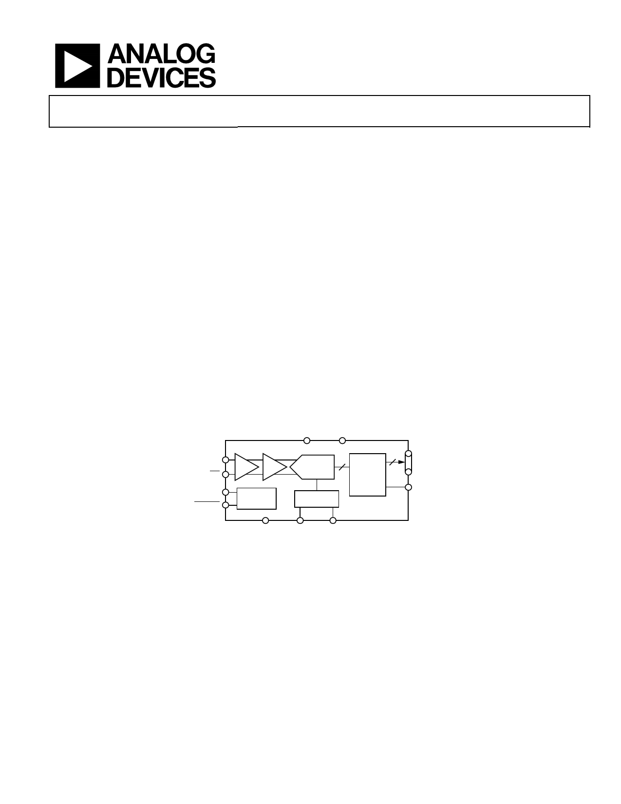
FUNCTIONAL BLOCK DIAGRAM
VCC
VDD
AIN
AIN
ENCODE
ENCODE
BUF
T/H
PIPELINE 12
ADC
12
OUTPUT
STAGING
TIMING
REF
AD9432
GND
VREFOUT VREFIN
Figure 1.
D11 TO D0
OR
Rev. F
Information furnished by Analog Devices is believed to be accurate and reliable. However, no
responsibility is assumed by Analog Devices for its use, nor for any infringements of patents or other
rights of third parties that may result from its use. Specifications subject to change without notice. No
license is granted by implication or otherwise under any patent or patent rights of Analog Devices.
Trademarksandregisteredtrademarksarethepropertyoftheirrespectiveowners.
One Technology Way, P.O. Box 9106, Norwood, MA 02062-9106, U.S.A.
Tel: 781.329.4700
www.analog.com
Fax: 781.461.3113 ©2002–2009 Analog Devices, Inc. All rights reserved.
1 page 
TIMING DIAGRAM
SAMPLE N – 1
AIN
ENCODE
SAMPLE N
tA
tEH
SAMPLE N + 10
SAMPLE N + 11
SAMPLE N + 1
tEL
SAMPLE N + 9
1/fS
ENCODE
D11 TO D0
DATA N – 11
DATA N – 10
DATA
N–9
DATA
N–2
tPD
DATA N – 1
DATA N
tV
DATA N + 1
Figure 2. Timing Diagram
AD9432
Rev. F | Page 5 of 16
5 Page 
TERMINOLOGY
Analog Bandwidth
The analog input frequency at which the spectral power of the
fundamental frequency (as determined by the FFT analysis) is
reduced by 3 dB.
Aperture Delay
The delay between a differential crossing of ENCODE and
ENCODE and the instant at which the analog input is sampled.
Aperture Uncertainty (Jitter)
The sample-to-sample variation in aperture delay.
Differential Nonlinearity (DNL)
The deviation of any code from an ideal 1 LSB step.
Effective Number of Bits (ENOB)
The effective number of bits (ENOB) is calculated from the
measured SNR based on the following equation:
ENOB =
SNR MEASURED
−1.76
dB + 20
log⎜⎜⎝⎛
Full − Scale Amplitude
Input Amplitude
⎟⎞
⎟⎠
6.02
Encode Pulse Width/Duty Cycle
Pulse width high is the minimum amount of time that the encode
pulse should be left in the Logic 1 state to achieve the rated per-
formance. Pulse width low is the minimum amount of time that
the encode pulse should be left in the Logic 0 state. At a given clock
rate, these specifications define an acceptable encode duty cycle.
Harmonic Distortion
The ratio of the rms signal amplitude fundamental frequency
to the rms signal amplitude of a single harmonic component
(second, third, and so on); reported in dBc.
Integral Nonlinearity (INL)
The deviation of the transfer function from a reference line
measured in fractions of 1 LSB using a “best straight line”
determined by a least square curve fit.
Maximum Conversion Rate
The maximum encode rate at which parametric testing is
performed.
Minimum Conversion Rate
The encode rate at which the SNR of the lowest analog signal
frequency drops by no more than 3 dB below the guaranteed
limit.
AD9432
Output Propagation Delay
The delay between a differential crossing of ENCODE and
ENCODE and the time when all output data bits are within
valid logic levels.
Power Supply Rejection Ratio (PSRR)
The ratio of a change in input offset voltage to a change in
power supply voltage.
Signal-to-Noise and Distortion (SINAD) Ratio
The ratio of the rms signal amplitude (set at 1 dB below full
scale) to the rms value of the sum of all other spectral compo-
nents, including harmonics but excluding dc.
Signal-to-Noise Ratio (SNR)
The ratio of the rms signal amplitude (set at 1 dB below full
scale) to the rms value of the sum of all other spectral com-
ponents, excluding the first five harmonics and dc.
Spurious-Free Dynamic Range (SFDR)
The ratio of the rms signal amplitude to the rms value of the
peak spurious spectral component. The peak spurious compo-
nent may or may not be a harmonic. May be reported in dBc
(degrades as signal level is lowered) or in dBFS (always related
back to converter full scale).
Two-Tone Intermodulation Distortion Rejection
The ratio of the rms value of either input tone (f1, f2) to the rms
value of the worst third-order intermodulation product;
reported in dBc. Products are located at 2f1 − f2 and 2f2 − f1.
Two-Tone SFDR
The ratio of the rms value of either input tone (f1, f2) to the rms
value of the peak spurious component. The peak spurious com-
ponent may or may not be an IMD product. May be reported in
dBc (degrades as signal level is lowered) or in dBFS (always
related back to converter full scale).
Worst Other Spur
The ratio of the rms signal amplitude to the rms value of the
worst spurious component (excluding the second-order and
third-order harmonic); reported in dBc.
Rev. F | Page 11 of 16
11 Page | ||
| Páginas | Total 16 Páginas | |
| PDF Descargar | [ Datasheet AD9432.PDF ] | |
Hoja de datos destacado
| Número de pieza | Descripción | Fabricantes |
| AD9430 | 3.3V A/D Converter | Analog Devices |
| AD9432 | 12-Bit/ 80 MSPS/105 MSPS A/D Converter | Analog Devices |
| AD9433 | IF Sampling ADC | Analog Devices |
| AD9434 | 1.8 V Analog-to-Digital Converter | Analog Devices |
| Número de pieza | Descripción | Fabricantes |
| SLA6805M | High Voltage 3 phase Motor Driver IC. |
Sanken |
| SDC1742 | 12- and 14-Bit Hybrid Synchro / Resolver-to-Digital Converters. |
Analog Devices |
|
DataSheet.es es una pagina web que funciona como un repositorio de manuales o hoja de datos de muchos de los productos más populares, |
| DataSheet.es | 2020 | Privacy Policy | Contacto | Buscar |