|
|
|
PDF AD7836 Data sheet ( Hoja de datos )
| Número de pieza | AD7836 | |
| Descripción | LC2MOS Quad 14-Bit DAC | |
| Fabricantes | Analog Devices | |
| Logotipo | ||
Hay una vista previa y un enlace de descarga de AD7836 (archivo pdf) en la parte inferior de esta página. Total 12 Páginas | ||
|
No Preview Available !
a
FEATURES
Four 14-Bit DACs in One Package
Voltage Outputs
Separate Offset Adjust for Each Output
Reference Range of ؎5 V
Maximum Output Voltage Range of ؎10 V
Clear Function to User-Defined Code
44-Pin MQFP Package
APPLICATIONS
Process Control
Automatic Test Equipment
General Purpose Instrumentation
LC2MOS
Quad 14-Bit DAC
AD7836
GENERAL DESCRIPTION
The AD7836 contains four 14-bit DACs on one monolithic
chip. It has output voltages with a full-scale range of ± 10 V
from reference voltages of ± 5 V.
The AD7836 accepts 14-bit parallel loaded data from the exter-
nal bus into one of the input latches under the control of the
WR, CS and DAC channel address pins, A0–A2.
The DAC outputs are updated individually, on reception of new
data. In addition, the SEL input can be used to apply the user
programmed value in DAC Register E to all DACs, thus setting
all DAC output voltages to the same level. The contents of the
DAC data registers are not affected by the SEL input.
Each DAC output is buffered with a gain of two amplifier into
which an external DAC offset voltage can be inserted via the
DUTGNDx pins.
The AD7836 is available in a 44-lead MQFP package.
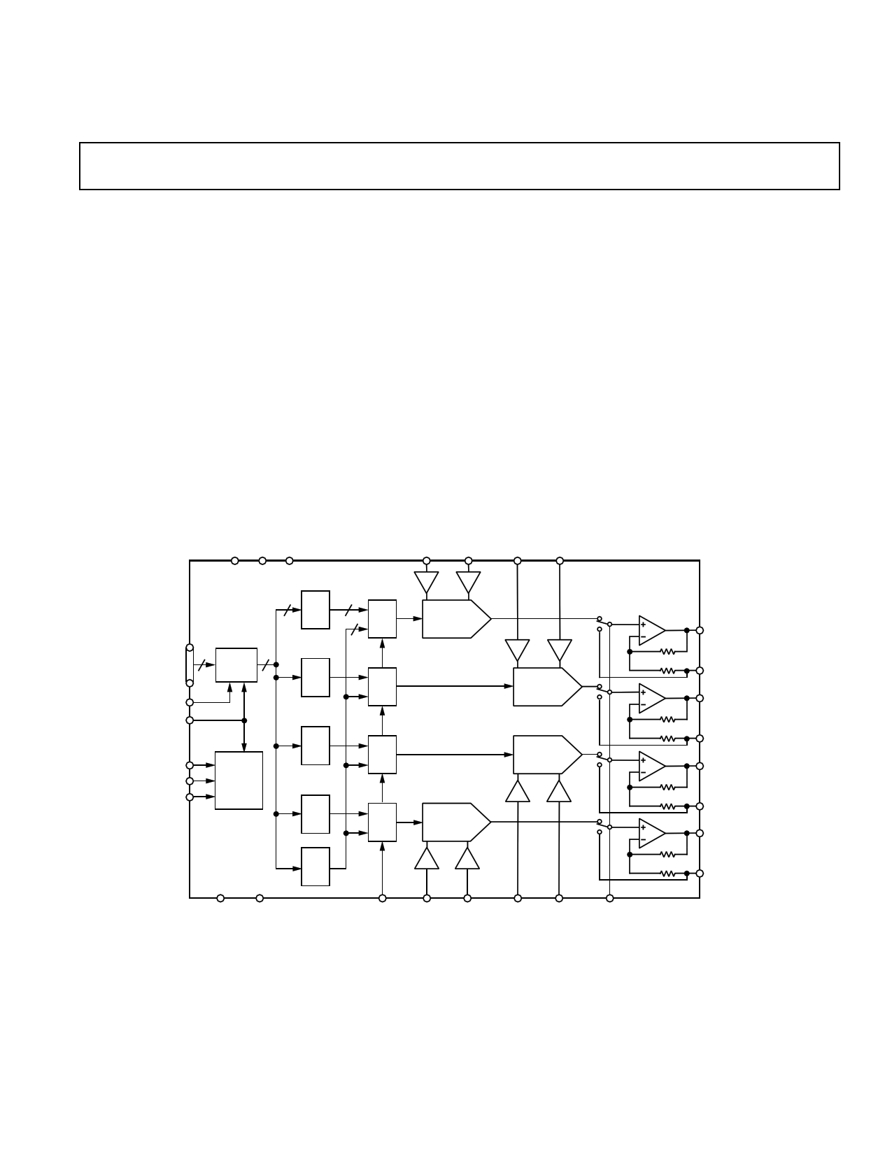
FUNCTIONAL BLOCK DIAGRAM
VCC VSS VDD
VREF(+)A VREF(–)A VREF(+)B VREF(–)B
AD7836
14 DATA 14
REG
A 14
MUX
DB13
DB0
WR
CS
14 14
INPUT
BUFFER
A0
A1
ADDRESS
DECODE
A2
DATA
REG
B
DATA
REG
C
DATA
REG
D
MUX
MUX
MUX
X1 X1
DAC A
DAC D
X1 X1
DAC B
DAC B
X1 X1
DGND AGND
DATA
REG
E
X1 X1
SEL VREF(+)D VREF(–)D VREF(+)C VREF(–)C CLR
VOUTA
R
R
DUTGND A
VOUTB
R
R
DUTGND B
VOUTC
R
R
DUTGND C
VOUTD
R
R
DUTGND D
REV. A
Information furnished by Analog Devices is believed to be accurate and
reliable. However, no responsibility is assumed by Analog Devices for its
use, nor for any infringements of patents or other rights of third parties
which may result from its use. No license is granted by implication or
otherwise under any patent or patent rights of Analog Devices.
One Technology Way, P.O. Box 9106, Norwood, MA 02062-9106, U.S.A.
Tel: 781/329-4700 World Wide Web Site: http://www.analog.com
Fax: 781/326-8703
© Analog Devices, Inc., 1999
1 page 
Pin Mnemonic
VCC
VSS
VDD
DGND
AGND
VREF(+)A, VREF(–)A
VREF(+)B, VREF(–)B
VREF(+)C, VREF(–)C
VREF(+)D, VREF(–)D
VOUTA . . . VOUTD
CS
DB0 . . . DB13
A0, A1, A2
CLR
WR
DUTGND A
DUTGND B
DUTGND C
DUTGND D
SEL
AD7836
Description
PIN DESCRIPTION
Logic Power Supply; +5 V ± 5%.
Negative Analog Power Supply; –15 V ± 5%.
Positive Analog Power Supply; +15 V ± 5%.
Digital Ground.
Analog Ground.
Reference Inputs for DAC A. These reference voltages are referred to AGND.
Reference Inputs for DAC B. These reference voltages are referred to AGND.
Reference Inputs for DAC C. These reference voltages are referred to AGND.
Reference Inputs for DAC D. These reference voltages are referred to AGND.
DAC Outputs.
Level-Triggered Chip Select Input (active low). The device is selected when this input is low.
Parallel Data Inputs. The AD7836 can accept a straight 14-bit parallel word on DB0 to DB13 where
DB13 is the MSB and DB0 is the LSB.
Address inputs. A0, A1 and A2 are decoded to select one of the five input latches for a data transfer.
Asynchronous Clear Input (level sensitive, active low). When this input is low, all analog outputs are
switched to the externally set potential on the DUTGND pin. The contents of data registers A to E are
not affected when the CLR pin is taken low. When CLR is brought back high, the DAC outputs revert
back to their original outputs as determined by the data in their data registers.
Level-Triggered Write Input (active low), when active and used in conjunction with CS to write data to
the AD7836 input buffer. Data is latched into the selected data register on the rising edge of WR.
Device Sense Ground for DAC A. Vout A is referenced to the voltage applied to this pin.
Device Sense Ground for DAC B. Vout B is referenced to the voltage applied to this pin.
Device Sense Ground for DAC C. Vout C is referenced to the voltage applied to this pin.
Device Sense Ground for DAC D. Vout D is referenced to the voltage applied to this pin.
Select pin, active high level triggered input. When the SEL input is high, the user programmed value in
DATAREG E will be loaded into all DAC registers and the DAC outputs updated accordingly. The con-
tents of the other DATA REGs (A–D) will not be affected by the SEL pin.
PIN CONFIGURATION
REV. A
33 32 31 30 29 28 27 26 25 24 23
VOUTC 34
VREF(–)C 35
VREF(+)C 36
AGND 37
NC 38
VDD 39
NC 40
VSS 41
VREF(+)A 42
VREF(–)A 43
VOUTA 44
AD7836
TOP VIEW
(Not to Scale)
PIN 1
IDENTIFIER
1 2 3 4 5 6 7 8 9 10 11
22 DB7
21 DB6
20 DB5
19 DB4
18 DB3
17 DB2
16 DB1
15 DB0
14 DGND
13 VCC
12 CLR
NC = NO CONNECT
–5–
5 Page 
AD7836
Automated Test Equipment
The AD7836 is particularly suited for use in an automated test
environment. Figure 21 shows the AD7836 providing the nec-
essary voltages for the pin driver and the window comparator in
a typical ATE pin electronics configuration. AD588s are used
to provide reference voltages for the AD7836. In the configu-
ration shown, the AD588s are configured so that the voltage at
Pin 1 is 5 V greater than the voltage at Pin 9 and the voltage at
Pin 15 is 5 V less than the voltage at Pin 9.
+15V –15V
VOFFSET
4
6
8
13
7
1F
2 16
3
1
AD588 15
14
VREF(+)A/B
VREF(–)A/B
VOUTA
9
10 11 12
VOUTB
DUTGND A/B
0.1F
AD7836*
+15V
PIN
DRIVER
–15V
+15V –15V
2 16
43
61
8
13
10
AD588
15
14
11
12
DUTGND C/D
VREF(+)C/D
VREF(–)C/D
VOUTC
VOUTD
AGND
DEVICE
GND
VOUT
DEVICE
GND
7
1F
8
DEVICE
GND
WINDOW
COMPARATOR
TO TESTER
*ADDITIONAL PINS OMITTED FOR CLARITY
Figure 21. ATE Application
One of the AD588s is used as a reference for DACs 1 and 2.
These DACs are used to provide high and low levels for the pin
driver. The pin driver may have an associated offset. This can
be nulled by applying an offset voltage to Pin 9 of the AD588.
First, the code 1000 . . . 0000 is loaded into the DACA latch
and the pin driver output is set to the DACA output. The
VOFFSET voltage is adjusted until 0 V appears between the pin
driver output and DUT GND. This causes both VREF(+) and
VREF(–) to be offset with respect to AGND by an amount equal
to VOFFSET. However, the output of the pin driver will vary
from –10 V to +10 V with respect to DUT GND as the DAC
input code varies from 000 . . . 000 to 111 . . . 111. The
VOFFSET voltage is also applied to the DUTGND pins. When a
clear is performed on the AD7836, the output of the pin driver
will be 0 V with respect to Device GND.
The other AD588 is used to provide a reference voltage for
DACs C and D. These provide the reference voltages for the
window comparator shown in the diagram. Note that Pin 9 of
this AD588 is connected to Device GND. This causes
VREF(+)C & D and VREF(–)C & D to be referenced to Device
GND. As DAC 3 and DAC 4 input codes vary from
000 . . . 000 to 111 . . . 111, VOUT3 and VOUT4 vary from –10 V
to +10 V with respect to Device GND. Device GND is also
connected to DUTGND. When the AD7836 is cleared,
VOUTC and VOUTD are cleared to 0 V with respect to DEVICE
GND.
TrimDAC is a registered trademark of Analog Devices, Inc.
Programmable Reference Generation for the AD7836 in an
ATE Application
The AD7836 is particularly suited for use in an automated test
environment. The reference input for the AD7836 quad 14-bit
DAC requires two references for each DAC. Programmable
references may be a requirement in some ATE applications as
the offset and gain errors at the output of each DAC can be ad-
justed by varying the voltages on the reference pins of the DAC.
To trim offset errors, the DAC is loaded with the digital code
000 . . . 000 and the voltage on the VREF(–) pin is adjusted until
the desired negative output voltage is obtained. To trim out
gain errors, first the offset error is trimmed. Then the DAC is
loaded with the code 111 . . . 111 and the voltage on the
VREF(+) pin is adjusted until the desired full scale voltage
minus one LSB is obtained.
It is not uncommon in ATE design, to have other circuitry at
the output of the AD7836 that can have offset and gain errors
of up to say ± 300 mV. These offset and gain errors can be eas-
ily removed by adjusting the reference voltages of the AD7836.
The AD7836 uses nominal reference values of ± 5 V to achieve
an output span of ± 10 V. Since the AD7836 has a gain of two
from the reference inputs to the DAC output, adjusting the ref-
erence voltages by ± 150 mV will adjust the DAC offset and
gain by ± 300 mV.
There are a number of suitable 8- and 10-bit DACs available
that would be suitable to drive the reference inputs of the
AD7836, such as the AD7804 which is a quad 10-bit digital-to-
analog converter with serial load capabilities. The voltage out-
put from this DAC is in the form of VBIAS ± VSWING and rail to
rail operation is achievable. The voltage reference for this DAC
can be internally generated or provided externally. This DAC
also contains an 8-bit SUB DAC which can be used to shift the
complete transfer function of each DAC around the VBIAS
point. This can be used as a fine trim on the output voltage. In
this Application two AD7804s are required to provide program-
mable reference capability for all four DACs. One AD7804 is
used to drive the VREF(+) pins and the second package used to
drive the VREF(–) pins.
Another suitable DAC for providing programmable reference
capability is the AD8803. This is an octal 8-bit trimDAC® and
provides independent control of both the top and bottom ends
of the trimDAC. This is helpful in maximizing the resolution of
devices with a limited allowable voltage control range.
The AD8803 has an output voltage range of GND to VDD (0 V to
+5 V). To trim the VREF(+) input, the appropriate trim range
on the AD8803 DAC can be set using the VREFL and VREFH
pins allowing 8 bits of resolution between the two points. This
will allow the VREF(+) pin to be adjusted to remove gain errors.
To trim the VREF(–) voltage, some method of providing a trim
voltage in the required negative voltage range is required. Nei-
ther the AD7804 or the AD8803 can provide this range in nor-
mal operation as their output range is 0 V to +5 V. There are
two methods of producing this negative voltage. One method is
to provide a positive output voltage and then to level shift that
analog voltage to the required negative range. Alternatively
REV. A
–11–
11 Page | ||
| Páginas | Total 12 Páginas | |
| PDF Descargar | [ Datasheet AD7836.PDF ] | |
Hoja de datos destacado
| Número de pieza | Descripción | Fabricantes |
| AD783 | Complete Very High Speed Sample-and-Hold Amplifier | Analog Devices |
| AD7834 | LC2MOS Quad 14-Bit DAC | Analog Devices |
| AD7835 | LC2MOS Quad 14-Bit DAC | Analog Devices |
| AD7836 | LC2MOS Quad 14-Bit DAC | Analog Devices |
| Número de pieza | Descripción | Fabricantes |
| SLA6805M | High Voltage 3 phase Motor Driver IC. |
Sanken |
| SDC1742 | 12- and 14-Bit Hybrid Synchro / Resolver-to-Digital Converters. |
Analog Devices |
|
DataSheet.es es una pagina web que funciona como un repositorio de manuales o hoja de datos de muchos de los productos más populares, |
| DataSheet.es | 2020 | Privacy Policy | Contacto | Buscar |