|
|
|
PDF AD7922 Data sheet ( Hoja de datos )
| Número de pieza | AD7922 | |
| Descripción | 2-Channel/ 2.35 V to 5.25 V/ 1 MSPS/ 10-/12-Bit ADCs | |
| Fabricantes | Analog Devices | |
| Logotipo | ||
1. AD7922 Hay una vista previa y un enlace de descarga de AD7922 (archivo pdf) en la parte inferior de esta página. Total 30 Páginas | ||
|
No Preview Available !
FEATURES
Fast throughput rate: 1 MSPS
Specified for VDD of 2.35 V to 5.25 V
Low power:
4.8 mW typ at 1 MSPS with 3 V supplies
15.5mW typ at 1 MSPS with 5 V supplies
Wide input bandwidth:
71 dB minimum SNR at 100 kHz input frequency
Flexible power/serial clock speed management
No pipeline delays
High speed serial interface:
SPI®/QSPI™/MICROWIRE™/DSP compatible
Standby mode: 1 µA maximum
Daisy-chain mode
8-lead TSOT package
8-lead MSOP package
APPLICATIONS
Battery-powered systems:
Personal digital assistants
Medical instruments
Mobile communications
Instrumentation and control systems
Data acquisition systems
High speed modems
Optical sensors
GENERAL DESCRIPTION
The AD7912/AD79221 are 10-bit and 12-bit, high speed, low
power, 2-channel successive approximation ADCs, respectively.
The parts operate from a single 2.35 V to 5.25 V power supply
and feature throughput rates of up to 1 MSPS. The parts contain
a low noise, wide bandwidth track-and-hold amplifier, which
can handle input frequencies in excess of 6 MHz.
The conversion process and data acquisition are controlled
using CS and the serial clock, allowing the devices to interface
with microprocessors or DSPs. The conversion rate is
determined by the SCLK signal. The input signal is sampled on
the falling edge of CS and the conversion is also initiated at this
point. The channel to be converted is selected through the DIN
pin, and the mode of operation is controlled by CS. The serial
data stream from the DOUT pin has a channel identifier bit and
mode identifier bit, which provide information about the
converted channel and the current mode of operation.
Rev. 0
Information furnished by Analog Devices is believed to be accurate and reliable.
However, no responsibility is assumed by Analog Devices for its use, nor for any
infringements of patents or other rights of third parties that may result from its use.
Specifications subject to change without notice. No license is granted by implication
or otherwise under any patent or patent rights of Analog Devices. Trademarks and
registered trademarks are the property of their respective owners.
2-Channel, 2.35 V to 5.25 V,
1 MSPS, 10-/12-Bit ADCs
AD7912/AD7922
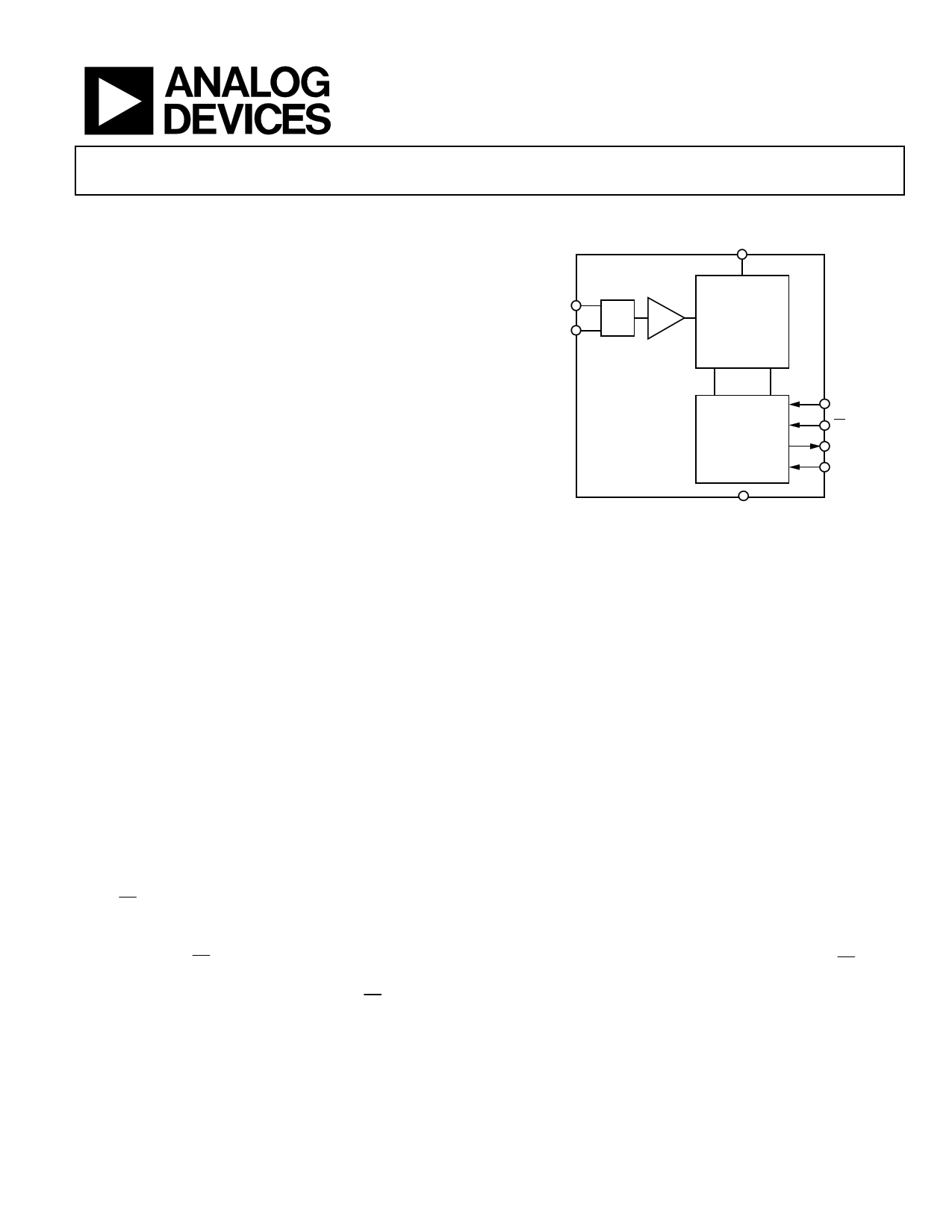
FUNCTIONAL BLOCK DIAGRAM
VDD
VIN0
VIN1
MUX
T/H
10-/12-BIT
SUCCESSIVE
APPROXIMATION
ADC
AD7912/AD7922 CONTROL LOGIC
SCLK
CS
DOUT
DIN
GND
Figure 1.
Several AD7912/AD7922 can be connected together in a daisy
chain. The AD7912/AD7922 feature a daisy-chain mode that
allows the user to read the conversion results from the ADCs
contained in the chain. The AD7912/AD7922 use advanced
design techniques to achieve very low power dissipation at high
throughput rates. The reference for the part is taken internally
from VDD, thereby allowing the widest dynamic input range to
the ADC.
PRODUCT HIGHLIGHTS
1. 2-channel, 1 MSPS, 10-/12-bit ADCs in TSOT package.
2. High throughput with low power consumption.
3. Flexible power/serial clock speed management.
The conversion rate is determined by the serial clock. The
parts also feature a power-down mode to maximize power
efficiency at lower throughput rates. Average power
consumption is reduced when the power-down mode is
used while not converting. Current consumption is 1 µA
maximum and 50 nA typically when in power-down mode.
4. Daisy-chain mode.
5. No pipeline delay.
The parts feature a standard successive approximation ADC
with accurate control of the sampling instant via a CS input
and once-off conversion control.
1 Protected by U.S. Patent Number 6,681,332.
One Technology Way, P.O. Box 9106, Norwood, MA 02062-9106, U.S.A.
Tel: 781.329.4700
www.analog.com
Fax: 781.326.8703 © 2004 Analog Devices, Inc. All rights reserved.
1 page 
AD7912/AD7922
AD7922 SPECIFICATIONS
Temperature range for A Grade from −40°C to +85°C.
VDD = 2.35 V to 5.25 V, fSCLK = 18 MHz, fSAMPLE = 1 MSPS; TA = TMIN to TMAX, unless otherwise noted.
Table 2.
Parameter
DYNAMIC PERFORMANCE
Signal-to-Noise + Distortion (SINAD)2
Signal-to-Noise Ratio (SNR)2
Total Harmonic Distortion (THD)2
Peak Harmonic or Spurious Noise (SFDR)2
Intermodulation Distortion (IMD)2
Second-Order Terms
Third-Order Terms
Aperture Delay
Aperture Jitter
Channel-to-Channel Isolation2
Full Power Bandwidth
DC ACCURACY
Resolution
Integral Nonlinearity2
Differential Nonlinearity2
Offset Error2
Offset Error Match2, 3
Gain Error2
Gain Error Match2, 3
Total Unadjusted Error (TUE)2
ANALOG INPUT
Input Voltage Ranges
DC Leakage Current
Input Capacitance
LOGIC INPUTS
Input High Voltage, VINH
Input Low Voltage, VINL
Input Current, IIN, SCLK Pin
Input Current, IIN, CS Pin
Input Current, IIN, DIN Pin
Input Capacitance, CIN3
A Grade1
70
72
71
72.5
−81
−84
−84
−86
10
30
90
8.5
1.5
12
±1.5
±0.7
−0.9/+1.5
−0.7/+1.2
±1
±0.1
±0.5
±0.02
±2
±0.5
±1
±0.2
±1.5
±0.5
0 to VDD
±0.3
20
0.7 (VDD)
2
0.3
0.2 (VDD)
0.8
±0.3
±0.3
±0.3
5
Unit
dB min
dB typ
dB min
dB typ
dB typ
dB typ
dB typ
dB typ
ns typ
ps typ
dB typ
MHz typ
MHz typ
Bits
LSB max
LSB typ
LSB max
LSB typ
LSB max
LSB typ
LSB max
LSB typ
LSB max
LSB typ
LSB max
LSB typ
LSB max
LSB typ
V
µA max
pF typ
V min
V min
V max
V max
V max
µA max
µA max
µA max
pF max
Test Conditions/Comments
fIN = 100 kHz sine wave
fa = 100.73 kHz, fb = 90.72 kHz
fa = 100.73 kHz, fb = 90.72 kHz
@ 3 dB
@ 0.1dB
VDD = 2.35 V to 3.6V
VDD = 4.75 V to 5.25V
Guaranteed no missed codes to 12 bits
VDD = 2.35 V to 3.6V
VDD = 4.75 V to 5.25V
VDD = 2.35 V to 3.6V
VDD = 4.75 V to 5.25V
VDD = 2.35 V to 3.6V
VDD = 4.75 V to 5.25V
VDD = 2.35 V to 3.6V
VDD = 4.75 V to 5.25V
VDD = 2.35 V to 3.6V
VDD = 4.75 V to 5.25V
VDD = 2.35 V to 3.6V
VDD = 4.75 V to 5.25V
2.35 V ≤ VDD ≤ 2.7 V
2.7 V < VDD ≤ 5.25 V
VDD = 2.35 V
2.35 V < VDD ≤ 2.7 V
2.7 V < VDD ≤ 5.25 V
Typically 8 nA, VIN = 0 V or VDD
Rev. 0 | Page 5 of 32
5 Page 
TERMINOLOGY
Integral Nonlinearity
The maximum deviation from a straight line passing through
the endpoints of the ADC transfer function. For the AD7912/
AD7922, the endpoints of the transfer function are zero scale, a
point 1 LSB below the first code transition, and full scale, a
point 1 LSB above the last code transition.
Differential Nonlinearity
The difference between the measured and the ideal 1 LSB
change between any two adjacent codes in the ADC.
Offset Error
The deviation of the first code transition (00…000) to
(00… 001) from the ideal, that is, AGND + 1 LSB.
Offset Error Match
The difference in offset error between any two channels.
Gain Error
The deviation of the last code transition (111…110) to
(111…111) from the ideal, that is, VDD − 1 LSB after the offset
error has been adjusted out.
Gain Error Match
The difference in gain error between any two channels.
Total Unadjusted Error
A comprehensive specification that includes gain error, linearity
error, and offset error.
Channel-to-Channel Isolation
A measure of the level of crosstalk between channels. It is
measured by applying a full-scale sine wave signal of 20 kHz to
500 kHz to the nonselected input channel and determining how
much that signal is attenuated in the selected channel with a
10 kHz signal. The figure is given worst case across both
channels for the AD7912/AD7922.
Track-and-Hold Acquisition Time
The time required for the output of the track-and-hold
amplifier to reach its final value within ±1 LSB after the end of
conversion. The track-and-hold amplifier returns to track mode
at the end of conversion. See the Serial Interface section for
more details.
AD7912/AD7922
Signal-to-Noise + Distortion Ratio (SINAD)
The measured ratio of signal-to-noise and distortion at the
output of the A/D converter. The signal is the rms value of the
sine wave, and noise is the rms sum of all nonfundamental
signals up to half the sampling frequency (fs/2), including
harmonics but excluding dc.
Signal-to-Noise Ratio (SNR)
The measured ratio of signal to noise at the output to the A/D
converter. The signal is the rms value of the sine wave input.
Noise is the rms quantization error within the Nyquist
bandwidth (fs/2). The rms value of a sine wave is one-half its
peak-to-peak value divided by √2, and the rms value for the
quantization noise is q/√12. The ratio is dependent on the
number of quantization levels in the digitization process; the
more levels, the smaller the quantization noise. For an ideal
N-bit converter, the SNR is defined as
SNR = 6.02 N + 1.76 dB
Therefore, for a 12-bit converter, SNR is 74 dB; for a 10-bit
converter, SNR is 62 dB.
However, various error sources in the ADC cause the measured
SNR to be less than the theoretical value. These errors occur due
to integral and differential nonlinearities, internal ac noise
sources, and so on.
Total Harmonic Distortion (THD)
The ratio of the rms sum of harmonics to the fundamental,
which is defined as
THD (dB) = 20 log V2 2 + V3 2 + V4 2 + V5 2 + V6 2
V1
where:
V1 is the rms amplitude of the fundamental.
V2, V3, V4, V5, and V6 are the rms amplitudes of the second
through the sixth harmonics.
Peak Harmonic or Spurious Noise
The ratio of the rms value of the next largest component in the
ADC output spectrum (up to fs /2 and excluding dc) to the rms
value of the fundamental. Normally, the value of this specifica-
tion is determined by the largest harmonic in the spectrum, but
for ADCs where the harmonics are buried in the noise floor, it is
a noise peak.
Rev. 0 | Page 11 of 32
11 Page | ||
| Páginas | Total 30 Páginas | |
| PDF Descargar | [ Datasheet AD7922.PDF ] | |
Hoja de datos destacado
| Número de pieza | Descripción | Fabricantes |
| AD7920 | 10-/12-Bit ADCs | Analog Devices |
| AD7921 | 10-/12-Bit ADCs | Analog Devices |
| AD7922 | 2-Channel/ 2.35 V to 5.25 V/ 1 MSPS/ 10-/12-Bit ADCs | Analog Devices |
| AD7923 | 200 kSPS 12-Bit ADC | Analog Devices |
| Número de pieza | Descripción | Fabricantes |
| SLA6805M | High Voltage 3 phase Motor Driver IC. |
Sanken |
| SDC1742 | 12- and 14-Bit Hybrid Synchro / Resolver-to-Digital Converters. |
Analog Devices |
|
DataSheet.es es una pagina web que funciona como un repositorio de manuales o hoja de datos de muchos de los productos más populares, |
| DataSheet.es | 2020 | Privacy Policy | Contacto | Buscar |