|
|
PDF AD587 Data sheet ( Hoja de datos )
| Número de pieza | AD587 | |
| Descripción | High Precision 10 V Reference | |
| Fabricantes | Analog Devices | |
| Logotipo |  |
|
Hay una vista previa y un enlace de descarga de AD587 (archivo pdf) en la parte inferior de esta página. Total 8 Páginas | ||
|
No Preview Available !
a
High Precision
10 V Reference
AD587
FEATURES
Laser Trimmed to High Accuracy:
10.000 V ؎5 mV (L and U Grades)
Trimmed Temperature Coefficient:
5 ppm/؇C max, (L and U Grades)
Noise Reduction Capability
Low Quiescent Current: 4 mA max
Output Trim Capability
MIL-STD-883 Compliant Versions Available
FUNCTIONAL BLOCK DIAGRAM
+VI N
2
NOISE
REDUCTION
8
RS
A1
RF
6 VOUT
RT
5 TRIM
RI
AD587
4
GND
NOTE:
PINS 1,3, AND 7 ARE INTERNAL TEST POINTS.
NO CONNECTIONS TO THESE POINTS.
PRODUCT DESCRIPTION
The AD587 represents a major advance in the state-of-the-art in
monolithic voltage references. Using a proprietary ion-implanted
buried Zener diode and laser wafer trimming of high stability
thin-film resistors, the AD587 provides outstanding perfor-
mance at low cost.
The AD587 offers much higher performance than most other
10 V references. Because the AD587 uses an industry standard
pinout, many systems can be upgraded instantly with the
AD587. The buried Zener approach to reference design pro-
vides lower noise and drift than bandgap voltage references. The
AD587 offers a noise reduction pin which can be used to further
reduce the noise level generated by the buried Zener.
The AD587 is recommended for use as a reference for 8-, 10-,
12-, 14- or 16-bit D/A converters which require an external
precision reference. The device is also ideal for successive
approximation or integrating A/D converters with up to 14 bits
of accuracy and, in general, can offer better performance than
the standard on-chip references.
The AD587J, K and L are specified for operation from 0°C to
+70°C, and the AD587S, T and U are specified for –55°C to
+125°C operation. All grades are available in 8-pin cerdip. The
J and K versions are also available in an 8-pin Small Outline IC
(SOIC) package for surface mount applications, while the J, K,
and L grades also come in an 8-pin plastic package.
PRODUCT HIGHLIGHTS
1. Laser trimming of both initial accuracy and temperature
coefficients results in very low errors over temperature with-
out the use of external components. The AD587L has a
maximum deviation from 10.000 V of ± 8.5 mV between 0°C
and +70°C, and the AD587U guarantees ± 14 mV maximum
total error between –55°C and +125°C.
2. For applications requiring higher precision, an optional fine
trim connection is provided.
3. Any system using an industry standard pinout 10 volt refer-
ence can be upgraded instantly with the AD587.
4. Output noise of the AD587 is very low, typically 4 µV p-p. A
noise reduction pin is provided for additional noise filtering
using an external capacitor.
5. The AD587 is available in versions compliant with MIL-
STD-883. Refer to the Analog Devices Military Products
Databook or current AD587/883B data sheet for detailed
specifications.
REV. D
Information furnished by Analog Devices is believed to be accurate and
reliable. However, no responsibility is assumed by Analog Devices for its
use, nor for any infringements of patents or other rights of third parties
which may result from its use. No license is granted by implication or
otherwise under any patent or patent rights of Analog Devices.
One Technology Way, P.O. Box 9106, Norwood, MA 02062-9106, U.S.A.
Tel: 781/329-4700 World Wide Web Site: http://www.analog.com
Fax: 781/326-8703
© Analog Devices, Inc., 2000
1 page 
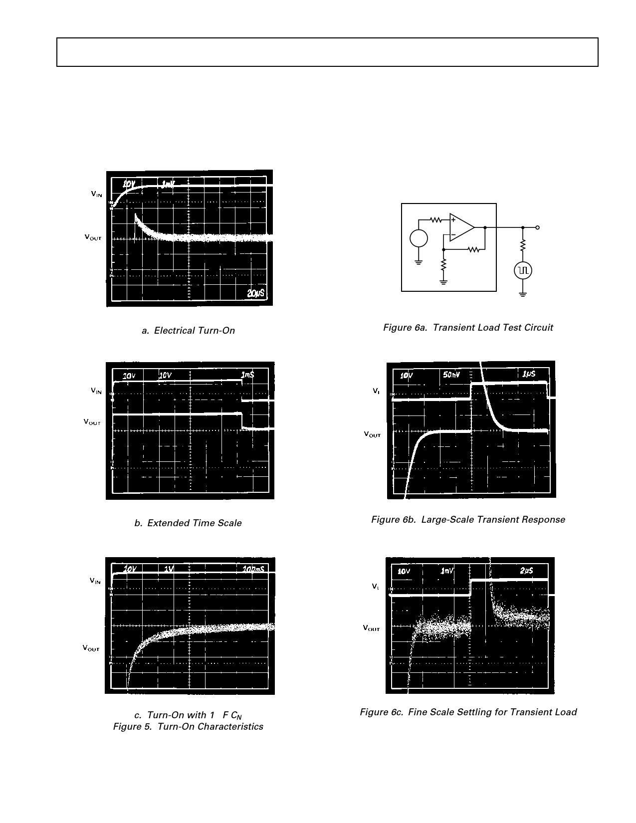
Output turn-on time is modified when an external noise reduc-
tion capacitor is used. When present, this capacitor acts as an
additional load to the internal Zener diode’s current source, re-
sulting in a somewhat longer turn-on time. In the case of a 1 µF
capacitor, the initial turn-on time is approximately 400 ms to
0.01% (see Figure 5c).
AD587
DYNAMIC PERFORMANCE
The output buffer amplifier is designed to provide the AD587
with static and dynamic load regulation superior to less com-
plete references.
Many A/D and D/A converters present transient current loads
to the reference, and poor reference response can degrade the
converter’s performance.
Figure 6 displays the characteristics of the AD587 output ampli-
fier driving a 0 mA to 10 mA load.
7.0V
VOUT
1kΩ
AD587
VL
10V
0V
a. Electrical Turn-On
Figure 6a. Transient Load Test Circuit
b. Extended Time Scale
Figure 6b. Large-Scale Transient Response
c. Turn-On with 1 µF CN
Figure 5. Turn-On Characteristics
Figure 6c. Fine Scale Settling for Transient Load
REV. D
–5–
5 Page | ||
| Páginas | Total 8 Páginas | |
| PDF Descargar | [ Datasheet AD587.PDF ] | |
Hoja de datos destacado
| Número de pieza | Descripción | Fabricantes |
| AD580 | High Precision 2.5 V IC Reference | Analog Devices |
| AD581 | High Precision 10 V IC Reference | Analog Devices |
| AD582 | Low Cost Sample/Hold Amplifier | Analog Devices |
| AD5821 | single 10-bit digital-to-analog converter | Analog Devices |
| Número de pieza | Descripción | Fabricantes |
| SLA6805M | High Voltage 3 phase Motor Driver IC. |
Sanken |
| SDC1742 | 12- and 14-Bit Hybrid Synchro / Resolver-to-Digital Converters. |
Analog Devices |
|
DataSheet.es es una pagina web que funciona como un repositorio de manuales o hoja de datos de muchos de los productos más populares, |
| DataSheet.es | 2020 | Privacy Policy | Contacto | Buscar |
