|
|
|
PDF AD6121 Data sheet ( Hoja de datos )
| Número de pieza | AD6121 | |
| Descripción | CDMA 3 V Receiver IF Subsystem with Integrated Voltage Regulator | |
| Fabricantes | Analog Devices | |
| Logotipo | ||
Hay una vista previa y un enlace de descarga de AD6121 (archivo pdf) en la parte inferior de esta página. Total 16 Páginas | ||
|
No Preview Available !
a
CDMA 3 V Receiver IF Subsystem
with Integrated Voltage Regulator
FEATURES
Fully Compliant with IS98A and PCS Specifications
CDMA, W-CDMA, AMPS, and TACS Operation
Linear IF Amplifier
5.9 dB Noise Figure
–47.5 dB to +47 dB Linear-in-dB Gain Control
Quadrature Demodulator
Demodulates IFs from 50 MHz to 350 MHz
Integral Low Dropout Regulator
200 mV Voltage Drop
Accepts 2.9 V to 4.2 V Input from Battery
Low Power
10 mA at Midgain
<1 A Sleep Mode Operation
Companion Transmitter IF Chip Available (AD6122)
APPLICATIONS
CDMA, W-CDMA, AMPS, and TACS Operation
QPSK Receivers
AD6121
GENERAL DESCRIPTION
The AD6121 is a low power receiver IF subsystem specifically
designed for CDMA applications. It consists of high dynamic
range IF amplifiers with voltage controlled gain, a divide-by-two
quadrature generator, an I and Q demodulator, and a power-
down control input. An integral low dropout regulator allows
operation from battery voltages from 2.9 V to 4.2 V.
The gain control input accepts an external gain control voltage
input from a DAC. It provides 94.5 dB of gain control with a
nominal 52.5 dB/V scale factor when using an internal voltage
reference. The gain control interface reference input can be
connected to either the internal reference or an external reference.
The I and Q demodulator provides differential quadrature base-
band outputs to interface with CDMA baseband converters. A
divide-by-two quadrature generator followed by dual polyphase
filters ensures maximum ± 2.5° quadrature accuracy.
The AD6121 IF Subsystem is fabricated using a 25 GHz ft
BiCMOS silicon process and is packaged in a 28-lead SSOP
and a 32-leadless LPCC chip scale package (5 mm × 5 mm).
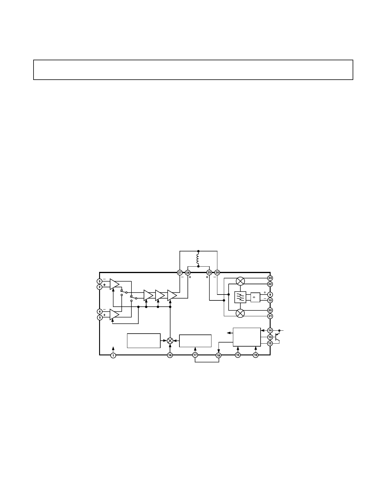
FUNCTIONAL BLOCK DIAGRAM
ROOFING
FILTER
CDMA
INPUT
FM
INPUT
IF
OUTPUT
DEMODULATOR
INPUT
IF AMPLIFIERS
INPUT STAGE
PTAT
TEMPERATURE
COMPENSATION
I
2
AD6121
Q
QUADRATURE DEMODULATOR
IOUT
IOUT
LOCAL
OSCILLATOR
INPUT
QOUT
QOUT
GAIN CONTROL
SCALE FACTOR
VREG
LOW
DROPOUT
REGULATOR
VPOS
CDMA/FM
SELECT
GAIN
CONTROL
VOLTAGE
INPUT
POWER- POWER-
GAIN
1.23V DOWN 2 DOWN 1
CONTROL REFERENCE
VOLTAGE OUTPUT
REFERENCE
INPUT
REV. B
Information furnished by Analog Devices is believed to be accurate and
reliable. However, no responsibility is assumed by Analog Devices for its
use, nor for any infringements of patents or other rights of third parties
which may result from its use. No license is granted by implication or
otherwise under any patent or patent rights of Analog Devices.
One Technology Way, P.O. Box 9106, Norwood, MA 02062-9106, U.S.A.
Tel: 781/329-4700 World Wide Web Site: http://www.analog.com
Fax: 781/326-8703
© Analog Devices, Inc., 2000
1 page 
Test Figures
AD6121
RF
SOURCE
AD6121
1: 8
110⍀ 10nF
CDMAIPP
IFOPP
10nF 453⍀
4:1
909⍀
110⍀
10nF
1k⍀
10nF 453⍀ 205⍀
TO
SPECTRUM
ANALYZER
CDMAIPN
IFOPN
INDUCTOR CHOSEN FOR PEAK RESPONSE
AT THE TEST FREQUENCY (SEE TEXT)
a. CDMA Input Port Characterization Impedance Match
RF
SOURCE
AD6121
453⍀ 10nF FMIPP
IFOPP
50⍀
10nF
FMIPN
IFOPN
b. FM Input Port Characterization Impedance Match
Figure 1. Quadrature Modulator Characterization Input and Output Impedance Matches
RF
SOURCE
1:4 453⍀ 10nF
DEMIPP
IOPP
205⍀ 453⍀ 10nF
DEMIPN
IOPN
LO
SOURCE
AD6121
QUADRATURE
DEMODULATOR
10nF
LOIPP
10nF
LOIPN
QOPP
QOPN
ALL SIGNAL PATHS MUST BE EQUAL
LENGTHS FOR I/Q MEASUREMENTS
+15V
0.1F
X1
X2 V–1
Y1
Y2 V–1
–15V
VP
OUT
A=1
VN AD830
0.1F
+15V
0.1F
X1
X2 V–1
Y1
Y2 V–1
–15V
VP
OUT
A=1
VN AD830
0.1F
50⍀
50⍀
Figure 2. IF Amplifier Characterization Input and Output Impedance Matches
I CHANNEL
Q CHANNEL
R&S
SMT03 RF
SYNC
REFERENCE
R&S
SMT03 RF
SYNC
REFERENCE
R&S
SMT03 RF
REV. B
CDMA
IN
IF OUT
AD6121
FM IN
DEMOD
IN
I CHANNEL
HPE3610
POWER SUPPLY
LO
INPUT Q CHANNEL
DC I/O
HP34970A
DATA ACQUISITION
& SWITCH CONTROL
ALL DC MEASUREMENT
AND CONTROL SIGNALS
Figure 3. General Test Set
–5–
CH1
HP8508A
VECTOR
VOLTMETER
CH2
R&S FSEA
SPECTRUM
RF INPUT ANALYZER
50⍀
TERMINATOR
5 Page 
AD6121
2CPAR
2CPAR
IFOPP
L/2
L/2
IFOPN
10nF
VCC
10nF
10nF
AD6121
the slope of the gain curve will change as a result of a change in
the required range for VGAIN. Figure 30 shows the piecewise
linear approximation of the gain curve for the AD6121.
MAXIMUM
GAIN
Figure 28. IF Amplifiers’ Output Configuration When
I and Q Demodulator Is Powered Down
In order to confirm whether the pull-up inductors have been
properly designed, sweep the IF frequency and view the output
of the IF amplifiers on a spectrum analyzer. If the inductor
value is correct, the signal should peak at the IF frequency.
The gain of the two amplifier sections (input stage followed by
amplifiers) changes sequentially for optimum signal-to-noise
ratio. For example, in CDMA mode, the gain of the CDMA
input amplifier first increases to maximum and then the gain of
the cascaded IF amplifiers increases to maximum. Likewise, when
decreasing gain, the gain of the cascaded amplifiers decreases to
minimum before the gain of the CDMA input amplifier.
The gain control circuits contain both temperature compensa-
tion circuitry and a choice of internal or external reference for
adjusting the gain scale factor. The gain control input accepts an
external gain control voltage from a DAC. It provides 94.5 dB
of gain control range with a nominal 52.5 dB/V scale factor.
Either an internal or external reference may be used to set the
gain control scale factor.
The external gain control input signal should be free of noise. In
a typical wireless application, it is recommended to filter this
signal in order to reduce the noise that results from the DAC
that generates it. A simple RC filter can be employed, but care
should be taken with its design. If too big a resistor is used, a
large voltage drop may occur across the resistor resulting in
lower gain than expected (as a result of a lower voltage reaching
the AD6121). An RC filter with a 1 kHz bandwidth, employing
a 1 kΩ resistor is appropriate. This results in a 150 nF capacitor.
The resulting circuit is shown in Figure 29.
FROM
BASEBAND
CONVERTER
1k⍀
150nF
AD6121
VGAIN
100k⍀
Figure 29. Gain Voltage Filtering
The AD6121’s overall gain, expressed in decibels, is linear in
dB with respect to the automatic gain control (AGC) voltage,
VGAIN. Either REFOUT, or an external reference voltage
connected to REFIN, may be used to set the voltage range for
VGAIN. When the internal 1.23 V reference, REFOUT, is
connected to REFIN, VGAIN will control the AGC range when
it is typically set between 0.5 V and 2.5 V. Minimum gain oc-
curs at minimum voltage on VGAIN and maximum gain occurs
at maximum voltage on VGAIN. The maximum and minimum
gain will not change with a change in voltage at REFIN. Rather,
MINIMUM
GAIN
VGAIN – Volts
Figure 30. Piecewise Linear Approximation for the
AD6121 Gain Curve
Because the minimum and maximum gains for the AD6121 are
constant, we can approximate the VGAIN range for a given
REFIN voltage by using Equation 2.
VGAIN = (GAIN – MinGain)×1.6 REFIN + 0.4 REFIN (2)
MaxGain – MinGain
Where MaxGain is the maximum gain (+47 dB) in dB, MinGain
is the minimum gain (–47.5 dB) in dB, REFIN is the reference
input voltage, in volts, VGAIN is the gain control voltage input,
in volts, and GAIN is the particular gain, in dB, we would have
for a given REFIN and VGAIN. Consequently, for any REFIN
we choose, we can calculate the VGAIN range by solving Equa-
tion 2 for VGAIN. For example, in order to determine the
VGAIN value for the maximum gain condition, given a 1.23 V
REFIN, we can solve Equation 2 for VGAIN by substituting
47 dB for GAIN and MaxGain, –47.5 dB for MinGain and
1.23 V for REFIN. VGAIN can then be calculated to be 2.46
V, or approximately 2.5 V. For the minimum gain condition,
we can determine the VGAIN value by substituting 47 dB for
MaxGain, –47.5 dB for Gain and MinGain and 1.23 V for
REFIN. VGAIN can then be calculated to be 0.492 V or ap-
proximately 0.5 V.
I and Q Demodulator
The I and Q demodulator provides differential quadrature base-
band outputs to CDMA baseband converters. The demodulator
provides 5.6 dB of voltage gain in addition to the gain provided
by the IF amplifier stage. The outputs of the I and Q demodula-
tor are filtered with a low-pass filter, which typically has a 16 MHz
bandwidth. A divide-by-two quadrature generator followed by
dual polyphase filters ensures a typical ± 1° quadrature accuracy
(Figure 31).
2 IF
LO INPUT
180
I
2
POLYPHASE
FILTERS
Q
2
I
QUADRATURE
OUTPUT TO
DEMODULATOR
Q
Figure 31. Simplified Quadrature Generator Circuit
REV. B
–11–
11 Page | ||
| Páginas | Total 16 Páginas | |
| PDF Descargar | [ Datasheet AD6121.PDF ] | |
Hoja de datos destacado
| Número de pieza | Descripción | Fabricantes |
| AD6121 | CDMA 3 V Receiver IF Subsystem with Integrated Voltage Regulator | Analog Devices |
| AD6122 | CDMA 3 V Transmitter IF Subsystem with Integrated Voltage Regulator | Analog Devices |
| Número de pieza | Descripción | Fabricantes |
| SLA6805M | High Voltage 3 phase Motor Driver IC. |
Sanken |
| SDC1742 | 12- and 14-Bit Hybrid Synchro / Resolver-to-Digital Converters. |
Analog Devices |
|
DataSheet.es es una pagina web que funciona como un repositorio de manuales o hoja de datos de muchos de los productos más populares, |
| DataSheet.es | 2020 | Privacy Policy | Contacto | Buscar |