|
|
|
PDF AD6458 Data sheet ( Hoja de datos )
| Número de pieza | AD6458 | |
| Descripción | GSM 3 V Receiver IF Subsystem | |
| Fabricantes | Analog Devices | |
| Logotipo | ||
Hay una vista previa y un enlace de descarga de AD6458 (archivo pdf) en la parte inferior de esta página. Total 12 Páginas | ||
|
No Preview Available !
a
FEATURES
Fully Compliant with Standard and Enhanced GSM
Specification
–12 dBm Input 1 dB Compression Point
–2 dBm Input Third Order Intercept
10 dB SSB Noise Figure (330 ⍀)
DC–400 MHz RF and LO Bandwidths
Linear IF Amplifier
Linear-in-dB and Stable over Temperature Voltage
Gain Control
Quadrature Demodulator
Onboard Phase-Locked Quadrature Oscillator
Demodulates IFs from 5 MHz to 50 MHz
Low Power
9 mA at Midgain
1 A Sleep Mode Operation
3.0 V to 3.6 V Operation
Interfaces to AD7013, AD7015 and AD6421 Baseband
Converters
20-Lead SSOP
GSM 3 V Receiver IF Subsystem
AD6458
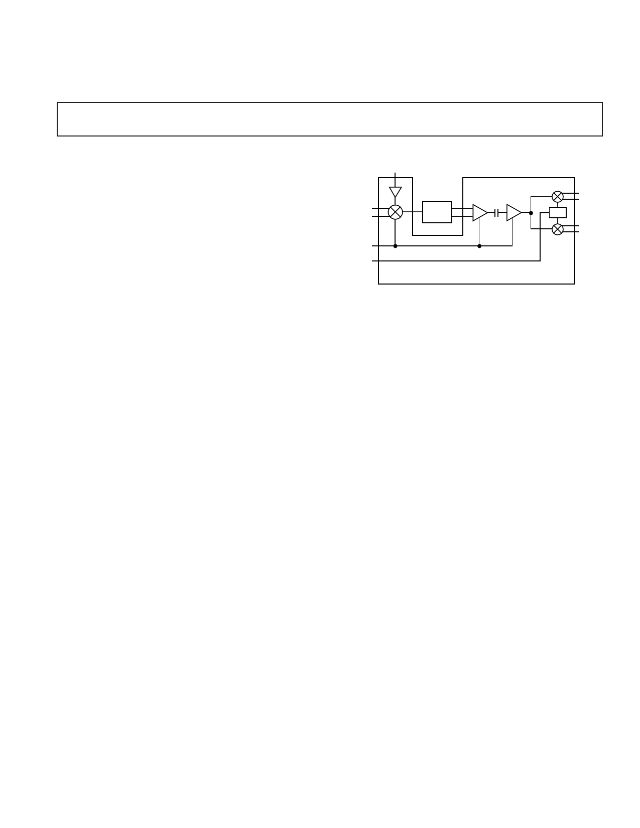
FUNCTIONAL BLOCK DIAGRAM
LO
RF
AGC
FREF
BPF
PLO
I
Q
AD6458
GENERAL DESCRIPTION
The AD6458 is a 3 V, low power receiver IF subsystem for
operation at input frequencies as high as 400 MHz and IFs from
5 MHz up to 50 MHz. It is optimized for operation in GSM,
DCS1800 and PCS1900 receivers. It consists of a mixer, IF
amplifier, I and Q demodulators, a phase-locked quadrature
oscillator, precise AGC subsystem, and a biasing system with
external power-down.
The low noise, high intercept mixer of the AD6458 is a
doubly-balanced Gilbert cell type. It has a nominal –12 dBm
input-referred 1 dB compression point and a –2 dBm input-
referred third-order intercept. The mixer section of the AD6458
also includes a local oscillator (LO) preamplifier, which lowers
the required LO drive to –16 dBm.
The gain control input accepts an external gain-control voltage
input from an external AGC detector or a DAC. It provides an
80 dB gain range with 27 mV/dB gain scaling.
The I and Q demodulators provide inphase and quadrature
baseband outputs to interface with Analog Devices’ AD7013
(IS54, TETRA, MSAT) and AD7015 and AD6421 (GSM,
DCS1800, PCS1900) baseband converters. An onboard
quadrature VCO which is externally phase-locked to the IF
signal drives the I and Q demodulators. This locked reference
signal is normally provided by an external VCTCXO under the
control of the radio’s digital processor. The AD6458 can also
provide demodulation of N-PSK and N-QAM in many non-
TDMA systems when used with external analog carrier recovery
systems such as the Costas Loop. Finally, the VCO can be
phase-locked to a frequency which is deliberately offset from the
IF, as in the case of a Beat-Frequency Oscillator (BFO), result-
ing in the product detection of CW or SSB.
The AD6458 uses supply voltages from 3.0 V to 3.6 V over the
temperature range of –40°C to +85°C. Operation is enabled by
a CMOS logical level; response time is typically <80 µs. When
disabled, the standby current is reduced to 1 µA.
The AD6458 comes in a 20-lead shrink small outline (SSOP)
surface-mount package.
REV. 0
Information furnished by Analog Devices is believed to be accurate and
reliable. However, no responsibility is assumed by Analog Devices for its
use, nor for any infringements of patents or other rights of third parties
which may result from its use. No license is granted by implication or
otherwise under any patent or patent rights of Analog Devices.
One Technology Way, P.O. Box 9106, Norwood, MA 02062-9106, U.S.A.
Tel: 617/329-4700 World Wide Web Site: http://www.analog.com
Fax: 617/326-8703
© Analog Devices, Inc., 1997
1 page 
HP8657B
10MHz OUT
10MHz IN
SYNC
IEEE
RF OUT
MOD I/O
SYNTHESIZER
HP8657B
10MHz OUT
10MHz IN
SYNC
IEEE
RF OUT
MOD I/O
SYNTHESIZER
HP8657B
10MHz OUT
10MHz IN
SYNC
IEEE
RF OUT
MOD I/O
SYNTHESIZER
DP8200
HI F
HI S
LO F
IEEE
LO S
GND
DC SOURCE
HP663X
IEEE
POWER
SUPPLY
HI
LO
HP34401
HI
LO IEEE
I HI
DMM
HP6237
+5V
–5V
COM
+15V
AD6458
PRUP
FREF
VPOS
VIN VP
LOIP
RFIP
AD6458
MOTHER BOARD
IOUT
QOUT
GREF
MXOP
GAIN
IFIN
HP8593E
CAL OUT
IEEE
RF I/P
28 VOLT
SWEEP OUT
ANALYSER
SPECTRUM
Figure 3. Mixer Characterization Setup
DP8200
HI F
HI S
LO F
LO S
IEEE
GND
DC SOURCE
REV. 0
FREF
LOIP
R2
50Ω
RFHI
R1
50Ω
GREF
C5
0.1µF
C2
1nF
C7
1nF
VPOS
C12
220pF
1 FREF
2 COM1
3 PRUP
C1
0.1µF
VSP1 20
FLTR 19
VSP2 18
R8 1kΩ
C10 1nF
4 LOIP
IRXP 17
C4 1nF
AD6458
5 RFLO
IRXN 16
6 RFHI
QRXP 15
7 COM2
QRXN 14
8 GREF
GAIN 13
9 MXOP
IFIM 12
10 IFIP 11
BPF2
C11
0.1µF
C13
10nF
R5
330Ω
PRUP
VPOS
IRXP
IRXN
QRXP
QRXN
C9
10nF
GAIN
Figure 4. Typical Connection Diagram
–5–
5 Page 
AD6458
VPOS
FROM
MIXER
CORE
MXP
MXM
160kΩ
VBIAS
275Ω
330Ω
MXOP
25kΩ 275Ω
Figure 32. Mixer Output Port
IF Amplifier
Most of the gain in the AD6458 resides in the IF amplifier strip,
which comprises two stages. Both are fully differential and each
has a gain span of 26 dB for the AGC voltage range of 0.2 V to
2.25 V. Thus, in conjunction with the variable gain of the mixer,
the total gain span is 76 dB. The overall IF gain varies from –9
dB to 48 dB for the nominal AGC voltage of 0.2 V to 2.25 V.
Maximum gain is at VGAIN = 0.2 V.
The IF input is differential at IFIP and IFIM. Figure 33 shows a
simplified schematic of the IF interface modeled as parallel RC
network.
The IF’s small-signal bandwidth is approximately 50 MHz from
IFIP and IFIM through the demodulator.
IFHI
IFLO
CSH
RSH
Figure 33. IF Amplifier Port Modeled as a Parallel RC
Network
Gain Scaling
The AD6458’s overall gain, expressed in decibels, is linear with
respect to the AGC voltage VGAIN at pin GAIN. The gain of all
sections is maximum when VGAIN is 0.2, and falls off as the bias
is increased to VGAIN = 2.25 and is independent of the power
supply voltage. The gain of all stages changes simultaneously.
The AD6458’s gain scaling is also temperature compensated.
The GAIN pin of the AD6458 is an input driven by an external
low impedance voltage source, normally a DAC, under the
control of radio’s digital processor.
The gain-control scaling is directly proportional to the reference
voltage applied to the pin GREF and is independent of the
power supply voltage. When this input is set to the nominal
value of 1.2 V, the scale is nominally 27 mV/dB (37 dB/V).
Under these conditions, 76 dB of gain range (mixer plus IF)
corresponds to a control voltage of 0.2 V <= VG <= 2.25 V. The
final centering of this 2.05 V range depends on the insertion
losses of the IF filters used.
Pin GREF can be tied to an external voltage reference, VREF,
provided, for example, by a AD1580 (1.21 V) voltage reference.
IRXP
IRXN
100pF
100pF
IRXP
IRXN
QRXP
QRXN
AD6458
100pF
GREF
GAIN
1nF
100pF
QRXP
QRXN
AD6421
0.1µF
160Ω
BREFOUT
BREFCAP
AGC DAC
FREF
VCTCXO
AFC DAC
Figure 34. Interfacing the AD6458 to the AD6421
Baseband Converter
When using the Analog Devices AD7013 (IS54, TETRA and
satellite receiver applications) and AD7015 or AD6421 (GSM,
DCS1800, PCS1900) baseband converters, the external ref-
erence may also be provided by the reference output of the
baseband converters. The interface between the AD6458 and
the AD6421 baseband converter is shown in Figure 34. The
AD6421 baseband converter provides a VREF of 1.23 V; an
auxiliary DAC in the AD6421 can be used to generate the AGC
voltage. Since it uses the same reference voltage, the numerical
input to this DAC provides an accurate RSSI value in digital
form, no longer requiring the reference voltage to have high
absolute accuracy.
I/Q Demodulators
Both demodulators (I and Q) receive their inputs internally
from the IF amplifiers. Each demodulator comprises a full-wave
synchronous detector followed by an 8 MHz, two-pole low-pass
filter, producing differential outputs at pins IRXP and IRXN,
and QRXP and QRXN. Using the I and Q demodulators for IFs
above 50 MHz is precluded by the 5 MHz to 50 MHz range of
the PLL used in the demodulator section.
The I and Q outputs are differential and can swing up to
2.2 V p-p at the low supply voltage of 3.0 V. They are nominally
centered at 1.5 V independently of power supply. They can
therefore directly drive the RX ADCs in the AD6421 baseband
converter, which require an amplitude of 1.23 V to fully load
them when driven by a differential signal. The conversion gain
of the I and Q demodulators is 17 dB.
For IFs of less than 8 MHz, the on-chip low-pass filters (8 MHz
cutoff) do not adequately attenuate the IF or feedthrough prod-
ucts; the maximum input voltage must thus be limited to allow
sufficient headroom at the I and Q outputs, not only for the de-
sired baseband signal but also the unattenuated higher order
demodulation products. These products can be removed by an
external low-pass filter. A simple 1-pole RC filter, with its cor-
ner above the modulation bandwidth, is sufficient to attenuate
undesired outputs. The design of the RC filter is eased by the
4.7 kΩ resistor integrated at each I and Q output pin.
REV. 0
–11–
11 Page | ||
| Páginas | Total 12 Páginas | |
| PDF Descargar | [ Datasheet AD6458.PDF ] | |
Hoja de datos destacado
| Número de pieza | Descripción | Fabricantes |
| AD645 | Low Noise/ Low Drift FET Op Amp | Analog Devices |
| AD6458 | GSM 3 V Receiver IF Subsystem | Analog Devices |
| AD6459 | GSM 3 V Receiver IF Subsystem | Analog Devices |
| Número de pieza | Descripción | Fabricantes |
| SLA6805M | High Voltage 3 phase Motor Driver IC. |
Sanken |
| SDC1742 | 12- and 14-Bit Hybrid Synchro / Resolver-to-Digital Converters. |
Analog Devices |
|
DataSheet.es es una pagina web que funciona como un repositorio de manuales o hoja de datos de muchos de los productos más populares, |
| DataSheet.es | 2020 | Privacy Policy | Contacto | Buscar |