|
|
|
PDF AD693 Data sheet ( Hoja de datos )
| Número de pieza | AD693 | |
| Descripción | Loop-Powered 4.20 mA Sensor Transmitter | |
| Fabricantes | Analog Devices | |
| Logotipo | ||
Hay una vista previa y un enlace de descarga de AD693 (archivo pdf) en la parte inferior de esta página. Total 12 Páginas | ||
|
No Preview Available !
a
FEATURES
Instrumentation Amplifier Front End
Loop-Powered Operation
Precalibrated 30 mV or 60 mV Input Spans
Independently Adjustable Output Span and Zero
Precalibrated Output Spans: 4–20 mA Unipolar
0–20 mA Unipolar
12 ؎ 8 mA Bipolar
Precalibrated 100 ⍀ RTD Interface
6.2 V Reference with Up to 3.5 mA of Current Available
Uncommitted Auxiliary Amp for Extra Flexibility
Optional External Pass Transistor to Reduce
Self-Heating Errors
Loop-Powered 4–20 mA
Sensor Transmitter
AD693
FUNCTIONAL BLOCK DIAGRAM
PRODUCT DESCRIPTION
The AD693 is a monolithic signal conditioning circuit which
accepts low-level inputs from a variety of transducers to control a
standard 4–20 mA, two-wire current loop. An on-chip voltage
reference and auxiliary amplifier are provided for transducer
excitation; up to 3.5 mA of excitation current is available when the
device is operated in the loop-powered mode. Alternatively, the
device may be locally powered for three-wire applications when
0–20 mA operation is desired.
Precalibrated 30 mV and 60 mV input spans may be set by
simple pin strapping. Other spans from 1 mV to 100 mV may
be realized with the addition of external resistors. The auxiliary
amplifier may be used in combination with on-chip voltages to
provide six precalibrated ranges for 100 Ω RTDs. Output span
and zero are also determined by pin strapping to obtain the
standard ranges: 4–20mA, 12 ± 8 mA and 0–20 mA.
Active laser trimming of the AD693’s thin-film resistors result
in high levels of accuracy without the need for additional
adjustments and calibration. Total unadjusted error is tested on
every device to be less than 0.5% of full scale at +25°C, and less
than 0.75% over the industrial temperature range. Residual
nonlinearity is under 0.05%. The AD693 also allows for the use
of an external pass transistor to further reduce errors caused by
self-heating.
For transmission of low-level signals from RTDs, bridges and
pressure transducers, the AD693 offers a cost-effective signal
conditioning solution. It is recommended as a replacement for
discrete designs in a variety of applications in process control,
factory automation and system monitoring.
The AD693 is packaged in a 20-pin ceramic side-brazed DIP,
20-pin Cerdip, and 20-pin LCCC and is specified over the
–40°C to +85°C industrial temperature range.
REV. A
Information furnished by Analog Devices is believed to be accurate and
reliable. However, no responsibility is assumed by Analog Devices for its
use, nor for any infringements of patents or other rights of third parties
which may result from its use. No license is granted by implication or
otherwise under any patent or patent rights of Analog Devices.
PRODUCT HIGHLIGHTS
1. The AD693 is a complete monolithic low-level voltage-to-
current loop signal conditioner.
2. Precalibrated output zero and span options include
4–20 mA, 0–20 mA, and 12 ± 8 mA in two- and three-wire
configurations.
3. Simple resistor programming adds a continuum of ranges
to the basic 30 mV and 60 mV input spans.
4. The common-mode range of the signal amplifier input
extends from ground to near the device’s operating voltage.
5. Provision for transducer excitation includes a 6.2 V
reference output and an auxiliary amplifier which may be
configured for voltage or current output and signal
amplification.
6. The circuit configuration permits simple linearization of
bridge, RTD, and other transducer signals.
7. A monitored output is provided to drive an external pass
transistor. This feature off-loads power dissipation to
extend the temperature range of operation, enhance
reliability, and minimize self-heating errors.
8. Laser-wafer trimming results in low unadjusted errors and
affords precalibrated input and output spans.
9. Zero and span are independently adjustable and noninteractive
to accommodate transducers or user defined ranges.
10. Six precalibrated temperature ranges are available with a
100 Ω RTD via pin strapping.
One Technology Way, P.O. Box 9106, Norwood, MA 02062-9106, U.S.A.
Tel: 617/329-4700
Fax: 617/326-8703
1 page 
AD693
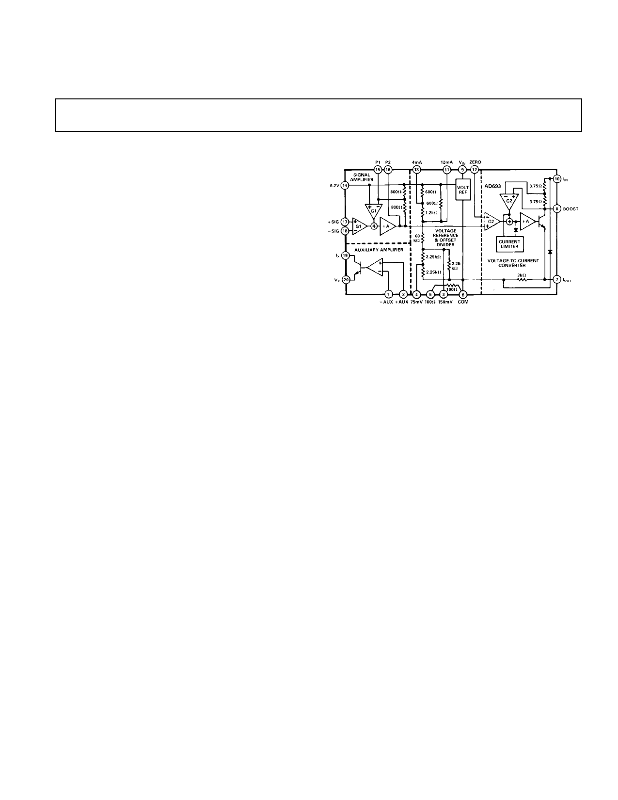
FUNCTIONAL DESCRIPTION
The operation of the AD693 can be understood by dividing the
circuit into three functional parts (see Figure 9). First, an
instrumentation amplifier front-end buffers and scales the low-
level input signal. This amplifier drives the second section, a V/I
converter, which provides the 4-to-20mA loop current. The
third section, a voltage reference and resistance divider, provides
application voltages for setting the various “live zero” currents.
In addition to these three main sections, there is an on-chip
auxiliary amplifier which can be used for transducer excitation.
VOLTAGE-TO-CURRENT (V/I) CONVERTER
The output NPN transistor for the V/I section sinks loop current
when driven on by a high gain amplifier at its base. The input for
this amplifier is derived from the difference in the outputs of the
matched preamplifiers having gains, G2. This difference is caused
to be small by the large gain, +A, and the negative feedback
through the NPN transistor and the loop current sampling resistor
between IIN and Boost. The signal across this resistor is compared
to the input of the left preamp and servos the loop current until
both signals are equal. Accurate voltage-to-current transformation
is thereby assured. The preamplifiers employ a special design
which allows the active feedback amplifier to operate from the most
positive point in the circuit, IIN.
The V/I stage is designed to have a nominal transconductance of
0.2666 A/V. Thus, a 75 mV signal applied to the inputs of the
V/I (Pin 16, noninverting; Pin 12, inverting) results in a
full-scale output current of 20 mA.
The current limiter operates as follows: the output of the feed-
back preamp is an accurate indication of the loop current. This
output is compared to an internal setpoint which backs off the
drive to the NPN transistor when the loop current approaches
25 mA. As a result, the loop and the AD693 are protected from the
consequences of voltage overdrive at the V/I input.
VOLTAGE REFERENCE AND DIVIDER
A stabilized bandgap voltage reference and laser-trimmed
resistor divider provide for both transducer excitation as well as
precalibrated offsets for the V/I converter. When not used for
external excitation, the reference should be loaded by approxi-
mately 1 mA (6.2 kΩ to common).
The 4 mA and 12 mA taps on the resistor divider correspond to
–15 mV and –45 mV, respectively, and result in a live zero of
4 mA or 12 mA of loop current when connected to the V/I
converter’s inverting input (Pin 12). Arranging the zero offset in
this way makes the zero signal output current independent of
input span. When the input to the signal amp is zero, the
noninverting input of the V/I is at 6.2 V.
Since the standard offsets are laser trimmed at the factory,
adjustment is seldom necessary except to accommodate the zero
offset of the actual source. (See “Adjusting Zero.”)
SIGNAL AMPLIFIER
The Signal Amplifier is an instrumentation amplifier used to
buffer and scale the input to match the desired span. Inputs
applied to the Signal Amplifier (at Pins 17 and 18) are amplified
and referred to the 6.2 V reference output in much the same way as
the level translation occurs in the V/I converter. Signals from the
two preamplifiers are subtracted, the difference is amplified, and
the result is fed back to the upper preamp to minimize the
difference. Since the two preamps are identical, this minimum will
occur when the voltage at the upper preamp just matches the
differential input applied to the Signal Amplifier at the left.
Since the signal which is applied to the V/I is attenuated across
the two 800 Ω resistors before driving the upper preamp, it will
necessarily be an amplified version of the signal applied between
Pins 17 and 18. By changing this attenuation, you can control
the span referred to the Signal Amplifier. To illustrate: a 75 mV
signal applied to the V/I results in a 20 mA loop current.
Nominally, 15 mV is applied to offset the zero to 4 mA leaving a
60 mV range to correspond to the span. And, since the nominal
attenuation of the resistors connected to Pins 16, 15 and 14 is
2.00, a 30 mV input signal will be doubled to result in 20 mA of
loop current. Shorting Pins 15 and 16 results in unity gain and
permits a 60 mV input span. Other choices of span may be
implemented with user supplied resistors to modify the
attenuation. (See section “Adjusting Input Span.”)
The Signal Amplifier is specially designed to accommodate a
large common-mode range. Common-mode signals anywhere up
to and beyond the 6.2 V reference are easily handled as long as
VIN is sufficiently positive. The Signal Amplifier is biased with
respect to VIN and requires about 3.5 volts of headroom. The
extended range will be useful when measuring sensors driven,
for example, by the auxiliary amplifier which may go above the
6.2 V potential. In addition, the PNP input stage will continue
to operate normally with common-mode voltages of several
hundred mV, negative, with respect to common. This feature
accommodates self-generating sensors, such as thermocouples,
which may produce small negative normal-mode signals as well
as common-mode noise on “grounded” signal sources.
Figure 9. Functional Flock Diagram
AUXILIARY AMPLIFIER
The Auxiliary Amplifier is included in the AD693 as a signal
conditioning aid. It can be used as an op amp in noninverting
applications and has special provisions to provide a controlled
current output. Designed with a differential input stage and an
unbiased Class A output stage, the amplifier can be resistively
loaded to common with the self-contained 100 Ω resistor or
with a user supplied resistor.
As a functional element, the Auxiliary Amplifier can be used in
dynamic bridges and arrangements such as the RTD signal
conditioner shown in Figure 17. It can be used to buffer, amplify
and combine other signals with the main Signal Amplifier. The
Auxiliary Amplifier can also provide other voltages for excitation
REV. A
–5–
5 Page 
AD693
Figure 19. Thermocouple Inputs with Cold Junction Compensation
Table II. Thermocouple Application—Cold Junction Compensation
POLARITY MATERIAL
AMBIENT
TYPE TEMP RCOMP RZ
30 mV 60 mV
TEMP TEMP
RANGE RANGE
+ IRON
– CONSTANTAN
J 25°
75°
51.7 Ω
53.6 Ω
301K
294K
546°C
1035°C
+ NICKEL-CHROME
25° 40.2 Ω 392K
721°C
—
_
NICKEL-ALUMINUM K 75°
42.2 Ω 374K
+ NICKEL-CHROME
25° 60.4 Ω 261K
E 413°C 787°C
– COPPER-NICKEL
75° 64.9 Ω 243K
+ COPPER
– COPPER-NICKEL
25°
T
75°
40.2 Ω
45.3 Ω
392K
USE WITH GAIN >2
340K
via a set of thermocouple tables referenced to °C. For example,
the output of a properly referenced type J thermocouple is
60 mV when the hot junction is at 1035°C. Table II lists the
maximum measurement temperature for several thermocouple
types using the preadjusted 30 mV and 60 mV input ranges.
More convenient temperature ranges can be selected by deter-
mining the full-scale input voltages via standard thermocouple
tables and adjusting the AD693 span. For example, suppose
only a 300°C span is to be measured with a type K thermo-
couple. From a standard table, the thermocouple output is
12.207 mV; since 60 mV at the signal amplifier corresponds to a
16 mA span at the output a gain of 5, or more precisely 60 mV/
12.207 mV = 4.915 will be needed. Using a 12.207 mV span in
the gain resistor formula given in “Adjusting Input Span” yields
a value of about 270 Ω as the minimum from P1 to 6.2 V. Adding
a 50 Ω potentiometer will allow ample adjustment range.
With the connection illustrated, the AD693 will give a full-scale
indication with an open thermocouple.
ERROR BUDGET ANALYSIS
Loop-Powered Operation specifications refer to parameters
tested with the AD693 operating as a loop-powered transmitter.
The specifications are valid for the preset spans of 30 mV,
60 mV and those spans in between. The section, “Components
of Error,” refers to parameters tested on the individual functional
blocks, (Signal Amplifier, V/I Converter, Voltage Reference, and
Auxiliary Amplifier). These can be used to get an indication of
device performance when the AD693 is used in local power
mode or when it is adjusted to spans of less than 30 mV.
Table III lists the expressions required to calculate the total
error. The AD693 is tested with a 250 Ω load, a 24 V loop supply
Table III. RTI Contributions to Span and Offset Error
RTI Contributions to Offset Error
Error Source
Expression for RTI Error at Zero
IZE Zero Current Error
IZE/XS
PSRR Power Supply Rejection Ratio (|VLOOP – 24 V| + [|RL – 250 Ω| × IZ]) × PSRR
CMRR Common-Mode Rejection Ratio |VCM – 3.1 V| × CMRR
IOS Input Offset Current
RS × IOS
RTI Contributions to Span Error
Error Source
XSE Transconductance Error
XPSRR Transconductance PSRR1
XCMRR Transconductance CMRR
XNL Nonlinearity
IDIFF Differential Input Current2
Expression for RTI Error at Full Scale
VSPAN × XSE
|RL – 250 Ω| × IS × PSRR
|VCM – 3.1 V| × VSPAN × XCMRR
VSPAN × XNL
RS × IDIFF
Abbreviations
IZ
IS
RS
RL
VLOOP
VCM
VSPAN
XS
Zero Current (usually 4 mA)
Output span (usually 16 mA)
Input source impedance
Load resistance
Loop supply voltage
Input common-mode voltage
Input span
Nominal transconductance in A/V
1The 4–20 mA signal, flowing through the metering resistor, modulates the power supplyvoltage seen
by the AD693. The change in voltage causes a power supply rejection error that varies with the
output current, thus it appears as a span error.
2The input bias current of the inverting input increases with input signal voltage. The differential
input current, IDIFF, equals the inverting input current minus the noninverting input current; see
Figure 2. IDIFF, flowing into an input source impedance, will cause an input voltage error that var-
ies with signal. If the change in differential input current with input signal is approximated as a
linear function, then any error due to source impedance may be approximated as a span error. To
calculate IDIFF, refer to Figure 2 and find the value for IDIFF/ + In corresponding to the full-scale
input voltage for your application. Multiply by + In max to get IDlFF. Multiply IDIFF by the source
impedance to get the input voltage error at full scale.
REV. A
–11–
11 Page | ||
| Páginas | Total 12 Páginas | |
| PDF Descargar | [ Datasheet AD693.PDF ] | |
Hoja de datos destacado
| Número de pieza | Descripción | Fabricantes |
| AD6905 | Baseband Processor for TD-HSDPA TD-SCDMA and GSM/GPRS/EGPRS | Analog Devices |
| AD693 | Loop-Powered 4.20 mA Sensor Transmitter | Analog Devices |
| AD694 | 4.20 mA Transmitter | Analog Devices |
| AD698 | Universal LVDT Signal Conditioner | Analog Devices |
| Número de pieza | Descripción | Fabricantes |
| SLA6805M | High Voltage 3 phase Motor Driver IC. |
Sanken |
| SDC1742 | 12- and 14-Bit Hybrid Synchro / Resolver-to-Digital Converters. |
Analog Devices |
|
DataSheet.es es una pagina web que funciona como un repositorio de manuales o hoja de datos de muchos de los productos más populares, |
| DataSheet.es | 2020 | Privacy Policy | Contacto | Buscar |