|
|
|
PDF AD722 Data sheet ( Hoja de datos )
| Número de pieza | AD722 | |
| Descripción | RGB to NTSC/PAL Encoder | |
| Fabricantes | Analog Devices | |
| Logotipo | ||
Hay una vista previa y un enlace de descarga de AD722 (archivo pdf) en la parte inferior de esta página. Total 12 Páginas | ||
|
No Preview Available !
a
RGB to NTSC/PAL Encoder
AD722
FEATURES
Low Cost, Integrated Solution
+5 V Operation
Accepts FSC Clock or Crystal, or 4FSC Clock
Composite Video and Separate Y/C (S-Video) Outputs
Minimal External Components:
No External Filters or Delay Lines Required
Onboard DC Restoration
Accepts Either HSYNC & VSYNC or CSYNC
Phase Lock to External Subcarrier
Drives 75 Ω Reverse-Terminated Loads
Logic Selectable NTSC or PAL Encoding Modes
Compact 16-Pin SOIC
APPLICATIONS
RGB to NTSC or PAL Encoding
PRODUCT DESCRIPTION
The AD722 is a low cost RGB to NTSC/PAL Encoder that
converts red, green and blue color component signals into their
corresponding luminance (baseband amplitude) and chromi-
nance (subcarrier amplitude and phase) signals in accordance
with either NTSC or PAL standards. These two outputs are
also combined to provide composite video output. All three out-
puts can simultaneously drive 75 Ω, reverse-terminated cables.
All logical inputs are CMOS compatible. The chip operates
from a single +5 V supply. No external delay lines or filters are
required. The AD722 may be powered down when not in use.
The AD722 accepts either FSC or 4FSC clock. When a clock is
not available, a low cost parallel-resonant crystal (3.58 MHz
(NTSC) or 4.43 MHz (PAL)) and the AD722’s on-chip oscilla-
tor generate the necessary subcarrier clock. The AD722 also ac-
cepts the subcarrier clock from an external video source.
The interface to VGA Controllers and MPEG Video Decoders
is simple: an on-chip logic “XNOR” accepts the available verti-
cal (VSYNC) and horizontal sync (HSYNC) signals and creates
the composite sync (CSYNC) signal on-chip. If available, the
AD722 will also accept a standard CSYNC signal by connecting
VSYNC to +5 V and applying CSYNC to HSYNC pin. The
AD722 contains decoding logic to identify valid HSYNC pulses
for correct burst insertion.
Delays in the U and V chroma filters are matched by an on-chip
sampled-data delay line in the Y signal path. To prevent
aliasing, a prefilter at 5 MHz is included ahead of the delay line
and a post-filter at 5 MHz is added after the delay line to sup-
press harmonics in the output. These low-pass filters are opti-
mized for minimum pulse overshoot. The overall luma delay,
relative to chroma, has been designed to be 170 ns, which
precompensates for delays in the filters used in the IF section of
a television receiver. This precompensation delay is already
present in TV broadcasts. The AD722 comes in a space-saving
SOIC and is specified for the 0°C to +70°C commercial tem-
perature range.
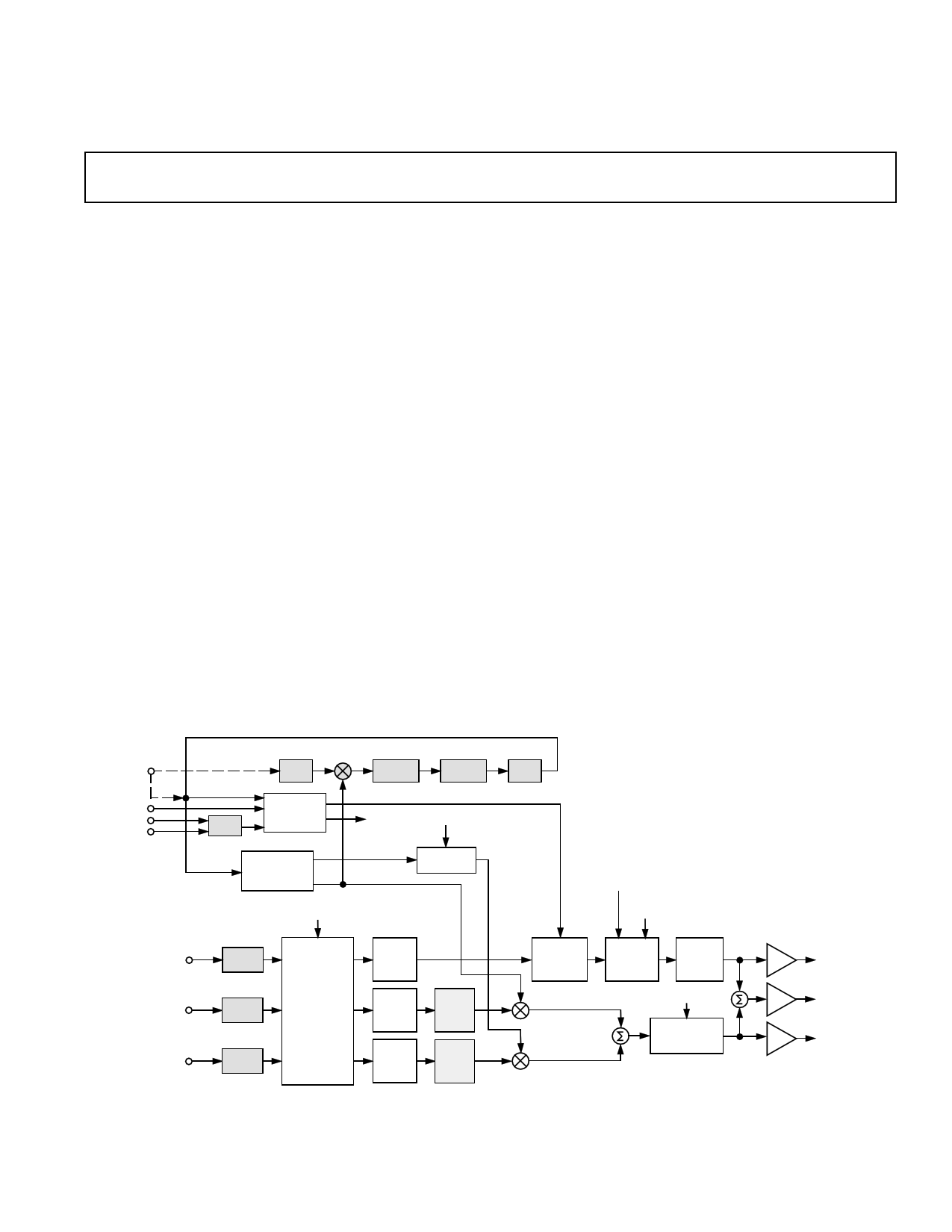
FUNCTIONAL BLOCK DIAGRAM
SUB-
CARRIER
FSC
4FSC
NTSC/PAL
HSYNC
VSYNC
XOSC
PHASE
DETECTOR
CHARGE
PUMP
FILTER
LOOP
4FSC
VCO
4FSC
XNOR
SYNC
SEPARATOR
FSC
BURST
CSYNC
NTSC/PAL
4FSC
CSYNC
QUADRATURE
+4
DECODER
FSC 90°
FSC 0°
±180°
SC 90°/270°
(PAL ONLY)
BURST
NTSC/PAL
CLOCK
AT 4FSC
RED
DC
CLAMP
GREEN
DC
CLAMP
Y 3-POLE
LP PRE-
FILTER
RGB-TO-YUV
ENCODING
U
4-POLE
MATRIX
LPF
U
CLAMP
BLUE
DC
CLAMP
V 4-POLE
LPF
V
CLAMP
REV. 0
Information furnished by Analog Devices is believed to be accurate and
reliable. However, no responsibility is assumed by Analog Devices for its
use, nor for any infringements of patents or other rights of third parties
which may result from its use. No license is granted by implication or
otherwise under any patent or patent rights of Analog Devices.
CSYNC
INSERTION
SAMPLED-
DATA
DELAY
LINE
2-POLE
LP POST-
FILTER
NTSC/PAL
BALANCED
MODULATORS
3-POLE LPF
3.6MHz (NTSC)
4.4MHz (PAL)
X2
LUMINANCE
OUTPUT
X2
COMPOSITE
OUTPUT
X2
CHROMINANCE
OUTPUT
© Analog Devices, Inc., 1995
One Technology Way, P.O. Box 9106, Norwood. MA 02062-9106, U.S.A.
Tel: 617/329-4700
Fax: 617/326-8703
1 page 
TEKTRONIX
TSG 300
COMPONENT
VIDEO
WAVEFORM
GENERATOR
COMPOSITE
SYNC
RGB 75Ω
3
GENLOCK
TEKTRONIX
1910
COMPOSITE
VIDEO
WAVEFORM
GENERATOR
FSC
AD722
RGB TO
NTSC/PAL
ENCODER
COMPOSITE
VIDEO
SONY
MONITOR
MODEL
1342
75Ω
TEKTRONIX
VM700A
WAVEFORM
MONITOR
Figure 1. Evaluation Setup
0.10
APL = 49.5%
525 LINE NTSC NO FILTERING
SLOW CLAMP TO 0.00V @ 6.63µs
0.5
100
50
0.0
–0.5
0
0
PRECISION MODE OFF
SYNCHRONOUS SYNC = SOURCE
FRAMES SELECTED : 1 2
–50
10 20 30 40 50 60
µs
Figure 2. Modulated Pulse and Bar, NTSC
Typical Characteristics–AD722
0.10
0.5
APL = 50.8%
525 LINE NTSC NO FILTERING
SLOW CLAMP TO 0.00V @ 6.63µs
100
50
0.0
–0.5
0
PRECISION MODE OFF
SYNCHRONOUS SYNC = SOURCE
FRAMES SELECTED : 1 2
10 20 30 40 50
µs
0
–50
60
Figure 4. 100% Color Bars, NTSC
0.10
0.5
APL = 50.6%
625 LINE PAL NO FILTERING
SLOW CLAMP TO 0.00V @ 6.72µs
0.0
–0.5
0
PRECISION MODE OFF SOUND-IN-SYNC OFF
SYNCHRONOUS SYNC = SOURCE
FRAMES SELECTED : 1 2 3 4
10 20 30 40 50
µs
60
Figure 5. 100% Color Bars, PAL
0.10
APL = 49.7%
625 LINE PAL NO FILTERING
SLOW CLAMP TO 0.00V @ 6.72µs
0.5
0.0
–0.5
0
PRECISION MODE OFF SOUND-IN-SYNC OFF
SYNCHRONOUS SYNC = SOURCE
FRAMES SELECTED : 1 2 3 4
10 20 30 40 50 60
µs
Figure 3. Modulated Pulse and Bar, PAL
Figure 6. 100% Color Bars on Vector Scope, NTSC
REV. 0
–5–
5 Page 
AD722
The IF strips used in TVs delay the chrominance by 170 ns
more than the luminance. To compensate for this, transmitted
video has the chrominance lead the luminance by 170 ns. The
term used for this is chrominance delay, and it is specified as
–170 ns, the negative (–) indicating that chrominance leads the
luminance. This correction to TV broadcasts was made in the
early days of TV and is the standard to this day.
The delay line used in the luminance path of the AD722 creates
a –170 ns chrominance delay. This will be realigned by the RF
section of a TV when it is used for receiving the signal.
However, for baseband inputs, the chrominance will lead the
luminance by a small amount. This will show up as a slight
color shadow to the left of objects. The physical offset can be
calculated by approximating the active horizontal line time of a
TV as 50 µs. Thus, the chrominance offset distance will be the
width of the screen times (50 µs/170 ns) or 0.0034. For a 13
inch monitor the screen width is about 10 in. (25 cm), so the
offset distance will be 0.034 in. (0.85 mm).
Dot Crawl
There are numerous distortions that are apparent in the presen-
tation of composite NTSC signals on TV monitors. These ef-
fects will vary in degree depending on the circuitry used by the
monitor to process the signal and on the nature of the image be-
ing displayed. It is generally not possible to produce pictures on
a composite monitor that are as high quality as those produced
by standard quality RGB, VGA monitors.
One well known distortion of composite video images is called
dot crawl. It shows up as a moving dot pattern at the interface
between two areas of different color. It is caused by the inability
of the monitor circuitry to adequately separate the luminance
and chrominance signals.
One way to prevent dot crawl is to use a video signal that has
separate luminance and chrominance. Such a signal is referred
to as S-video or Y/C video. Since the luminance and chromi-
nance are already separated, the monitor does not have to per-
form this function. The S-Video outputs of the AD722 can be
used to create higher quality pictures when there is an S-Video
input available on the monitor.
Flicker
In a VGA conversion application, where the software controlled
registers are correctly set, there are two techniques that are com-
monly used by VGA controller manufacturers to generate the
interlaced signal. Each of these techniques introduces a unique
characteristic into the display created by the AD722. The arti-
facts described below are not due to the encoder or its encoding
algorithm as all encoders will generate the same display when
presented with these inputs. They are due to the method used
by the controller display chip to convert a noninterlaced output
to an interlaced signal. The method used is a feature of the de-
sign of the VGA chip and is not programmable.
The first interlacing technique outputs a true interlaced signal
with odd and even fields (one each to a frame Figure 17a). This
provides the best picture quality when displaying photography,
CD video and animation (games, etc.). However, it will intro-
duce a defect commonly referred to as flicker into the display.
Flicker is a fundamental defect of all interlaced displays and is
caused by the alternating field characteristic of the interlace
technique. Consider a one pixel high black line which extends
horizontally across a white screen. This line will exist in only
one field and will be refreshed at a rate of 30 Hz (25 Hz for
PAL). During the time that the other field is being displayed the
line will not be displayed. The human eye is capable of detect-
ing this, and the display will be perceived to have a pulsating or
flickering black line. This effect is highly content sensitive and
is most pronounced in applications in which text and thin
horizontal lines are present. In applications such as CD video,
photography and animation, portions of objects naturally
occur in both odd and even fields and the effect of flicker is
imperceptible.
The second technique which is commonly used is to output an odd
and even field which are identical (Figure 17b). This ignores the
data which naturally occurs in one of the fields. In this case the
same one pixel high line mentioned above would either appear
as a two pixel high line, (one pixel high in both the odd and even
field) or will not appear at all if it is in the data which is ignored by
the controller. Which of these cases occurs is dependent on the
placement of the line on the screen. This technique provides a
stable (i.e., nonflickering) display for all applications, but small
text can be difficult to read and lines in drawings (or spread-
sheets) can disappear. As above, graphics and animation are not
particularly affected although some resolution is lost.
There are methods to dramatically reduce the effect of flicker and
maintain high resolution. The most common is to ensure that dis-
play data never exists solely in a single line. This can be accom-
plished by averaging/weighting the contents of successive/multiple
noninterlaced lines prior to creating a true interlaced output (Fig-
ure 17c). In a sense this provides an output which will lie between
the two extremes described above. The weight or percentage of one
line that appears in another and the number of lines used are vari-
ables that must be considered in developing a system of this type. If
this type of signal processing is performed, it must be completed
prior to the data being presented to the AD722 for encoding.
Vertical Scaling
In addition to converting the computer generated image from
noninterlaced to interlaced format, it is also necessary to scale
the image down to fit into NTSC or PAL format. The most
common vertical lines/screen for VGA display are 480 and 600
lines. NTSC can only accommodate approximately 400 visible
lines/frame (200 per field), PAL can accommodate 576 lines/
frame (288 per field). If scaling is not performed, portions of
the original image will not appear in the television display.
This line reduction can be performed by merely eliminating ev-
ery Nth (6th line in converting 480 lines to NSTC or every 25th
line in converting 600 lines to PAL). This risks generation of
jagged edges and jerky movement. It is best to combine the scaling
with the interpolation/averaging technique discussed above to
ensure that valuable data is not arbitrarily discarded in the scaling
process. Like the flicker reduction technique mentioned above,
the line reduction must be accomplished prior to the AD722 en-
coding operation.
There is a new generation of VGA controllers on the market
specifically designed to utilize these techniques to provide a
crisp and stable display for both text and graphics oriented ap-
plications. In addition these chips rescale the output from the
computer to fit correctly on the screen of a television. A list of
known devices is available through Analog Devices’ Applications
group, but the most complete and current information will be
available from the manufacturers of graphics controller ICs.
REV. 0
–11–
11 Page | ||
| Páginas | Total 12 Páginas | |
| PDF Descargar | [ Datasheet AD722.PDF ] | |
Hoja de datos destacado
| Número de pieza | Descripción | Fabricantes |
| AD720 | RGB to NTSC/PAL Encoders | Analog Devices |
| AD721 | RGB to NTSC/PAL Encoders | Analog Devices |
| AD7216N2L | AC-DC / External Freestanding Adapter | Emerson |
| AD722 | RGB to NTSC/PAL Encoder | Analog Devices |
| Número de pieza | Descripción | Fabricantes |
| SLA6805M | High Voltage 3 phase Motor Driver IC. |
Sanken |
| SDC1742 | 12- and 14-Bit Hybrid Synchro / Resolver-to-Digital Converters. |
Analog Devices |
|
DataSheet.es es una pagina web que funciona como un repositorio de manuales o hoja de datos de muchos de los productos más populares, |
| DataSheet.es | 2020 | Privacy Policy | Contacto | Buscar |