|
|
|
PDF AD7237A Data sheet ( Hoja de datos )
| Número de pieza | AD7237A | |
| Descripción | LC2MOS Dual 12-Bit DACPORTs | |
| Fabricantes | Analog Devices | |
| Logotipo | ||
Hay una vista previa y un enlace de descarga de AD7237A (archivo pdf) en la parte inferior de esta página. Total 12 Páginas | ||
|
No Preview Available !
a
FEATURES
Complete Dual 12-Bit DAC Comprising
Two 12-Bit CMOS DACs
On-Chip Voltage Reference
Output Amplifiers
Reference Buffer Amplifiers
Improved AD7237/AD7247:
12 V to 15 V Operation
Faster Interface –30 ns typ Data Setup Time
Parallel Loading Structure: AD7247A
(8+4) Loading Structure: AD7237A
Single or Dual Supply Operation
Low Power—165 mW typ in Single Supply
LC2MOS
Dual 12-Bit DACPORTs
AD7237A/AD7247A
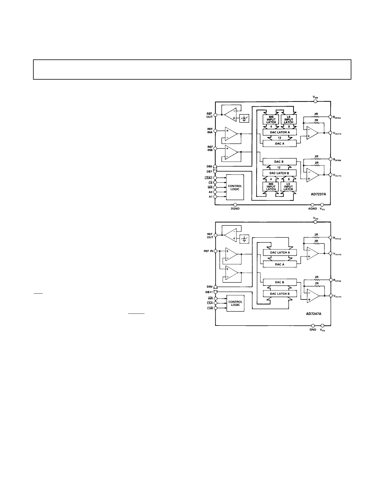
FUNCTIONAL BLOCK DIAGRAMS
GENERAL DESCRIPTION
The AD7237A/AD7247A is an enhanced version of the industry
standard AD7237/AD7247. Improvements include operation
from 12 V to 15 V supplies, faster interface times and better
reference variations with VDD. Additional features include faster
settling times.
The AD7237A/AD7247A is a complete, dual, 12-bit, voltage
output digital-to-analog converter with output amplifiers and
Zener voltage reference on a monolithic CMOS chip. No exter-
nal user trims are required to achieve full specified performance.
Both parts are microprocessor compatible, with high speed data
latches and interface logic. The AD7247A accepts 12-bit paral-
lel data which is loaded into the respective DAC latch using the
WR input and a separate Chip Select input for each DAC. The
AD7237A has a double buffered interface structure and an 8-bit
wide data bus with data loaded to the respective input latch in
two write operations. An asynchronous LDAC signal on the
AD7237A updates the DAC latches and analog outputs.
A REF OUT/REF IN function is provided which allows either
the on-chip 5 V reference or an external reference to be used as
a reference voltage for the part. For single supply operation, two
output ranges of 0 V to +5 V and 0 V to +10 V are available,
while these two ranges plus an additional ± 5 V range are avail-
able with dual supplies. The output amplifiers are capable of de-
veloping +10 V across a 2 kΩ load to GND.
The AD7237A/AD7247A is fabricated in Linear Compatible
CMOS (LC2MOS), an advanced, mixed technology process
that combines precision bipolar circuits with low power CMOS
logic. Both parts are available in a 24-pin, 0.3" wide plastic and
hermetic dual-in-line package (DIP) and are also packaged in a
24-lead small outline (SOIC) package.
REV. 0
Information furnished by Analog Devices is believed to be accurate and
reliable. However, no responsibility is assumed by Analog Devices for its
use, nor for any infringements of patents or other rights of third parties
which may result from its use. No license is granted by implication or
otherwise under any patent or patent rights of Analog Devices.
PRODUCT HIGHLIGHTS
1. The AD7237A/AD7247A is a dual 12-bit DACPORT® on a
single chip. This single chip design and small package size
offer considerable space saving and increased reliability over
multichip designs.
2. The improved interface times of the parts allow easy, direct
interfacing to most modern microprocessors, whether they
have 8-bit or 16-bit data bus structures.
3. The AD7237A/AD7247A features a wide power supply
range allowing operation from 12 V supplies.
DACPORT is a registered trademark of Analog Devices, Inc.
One Technology Way, P.O. Box 9106, Norwood, MA 02062-9106, U.S.A.
Tel: 617/329-4700
Fax: 617/326-8703
1 page 
AD7237A/AD7247A
AD7247A PIN FUNCTION DESCRIPTION (DIP PIN NUMBERS)
Pin Mnemonic Description
1
2
3
4
5
6
7–15
16
17
18
19
20
21
22
23
24
REF OUT
ROFSB
VOUTB
DB11
DB10
GND
DB9-DB1
DB0
CSB
CSA
WR
VDD
VOUTA
VSS
ROFSA
REF IN
Voltage Reference Output. The internal 5 V analog reference is provided at this pin. To operate the part
with internal reference, REF OUT should be connected to REF IN.
Output Offset Resistor for DAC B. This input configures the output ranges for DAC B. It is connected to
VOUTB for the +5 V range, to GND for the +10 V range and to REF IN for the ± 5 V range.
Analog Output Voltage from DAC B. This is the buffer amplifier output voltage. Three different output
voltage ranges can be chosen: 0 V to +5 V, 0 V to +10 V and ± 5 V. The amplifier is capable of developing
+10 V across a 2 kΩ resistor to GND.
Data Bit 11 (MSB).
Data Bit 10.
Ground. Ground reference for all on-chip circuitry.
Data Bit 9 to Data Bit 1.
Data Bit 0 (LSB).
Chip Select Input for DAC B. Active low logic input. DAC B is selected when this input is active.
Chip Select Input for DAC A. Active low logic input. DAC A is selected when this input is active.
Write Input. WR is an active low logic input which is used in conjunction with CSA and CSB to write data
to the DAC latches.
Positive Supply (+12 V to +15 V).
Analog Output Voltage from DAC A. This is the buffer amplifier output voltage. Three different output
voltage ranges can be chosen: 0 V to +5 V, 0 V to +10 V and ± 5 V. The amplifier is capable of developing
+10 V across a 2 kΩ resistor to GND.
Negative Supply (0 V or –12 V to –15 V).
Output Offset Resistor for DAC A. This input configures the output ranges for DAC A. It is connected to
VOUTA for the +5 V range, to GND for the +10 V range and to REF IN for the ± 5 V range.
Voltage Reference Input. The common reference voltage for both DACs is applied to this pin. It is internally
buffered before being applied to both DACs. The nominal reference voltage for correct operation of the
AD7247A is 5 V.
AD7237A PIN CONFIGURATION
DIP and SOIC
AD7247A PIN CONFIGURATION
DIP and SOIC
REV. 0
–5–
5 Page 
MICROPROCESSOR INTERFACING—AD7247A
Figures 10 to 12 show interfaces between the AD7247A and
the ADSP-2101 DSP processor and the 8086 and 68000 16-bit
microprocessors. In all three interfaces, the AD7247A is
memory-mapped with a separate memory address for each DAC.
AD7247A—ADSP-2101 Interface
Figure 10 shows an interface between the AD7247A and the
ADSP-2101. The 12-bit word is written to the selected DAC
latch of the AD7247A in a single instruction, and the analog
output responds immediately. Depending on the clock fre-
quency of the ADSP-2101, either one or two wait states will
have to be programmed into the data memory wait state control
register of the ADSP-2101.
AD7237A/AD7247A
AD7247A—MC68000 Interface
Interfacing between the AD7247A and the MC68000 micropro-
cessor is achieved using the circuit of Figure 12. Once again, the
12-bit word is written to the selected DAC latch of the
AD7247A in a single MOVE instruction. CSA and CSB have to
be AND-gated to provide a DTACK signal for the MC68000
when either DAC latch is selected.
Figure 10. AD7247A to ADSP-2101 Interface
AD7247A—8086 Interface
Figure 11 shows an interface between the AD7247A and the
8086 microprocessor. The 12-bit word is written to the selected
DAC latch of the AD7247A in a single MOV instruction, and
the analog output responds immediately.
Figure 12. AD7247A to MC68000 Interface
MICROPROCESSOR INTERFACING—AD7237A
Figures 13 to 15 show the AD7237A configured for interfacing
to microprocessors with 8-bit databus systems. In all cases, data
is right-justified, and the AD7237A is memory-mapped with the
two lowest address lines of the microprocessor address bus driv-
ing the A0 and A1 inputs of the converter.
AD7237A—8085A/8088 Interface
Figure 13 shows the connection diagram for interfacing the
AD7237A to both the 8085A and the 8088. This scheme is also
suited to the Z80 microprocessor, but the Z80 address/ databus
does not have to be demultiplexed. The AD7237A requires five
separate memory addresses, one for the each MS latch and one
for each LS latch and one for the common LDAC input. Data is
written to the respective input latch in two write operations.
Figure 11. AD7247A to 8086 Interface
Figure 13. AD7237A to 8085A/8088 Interface
REV. 0
–11–
11 Page | ||
| Páginas | Total 12 Páginas | |
| PDF Descargar | [ Datasheet AD7237A.PDF ] | |
Hoja de datos destacado
| Número de pieza | Descripción | Fabricantes |
| AD7237 | LC2MOS DUAL 12-BIT DACPORT | Analog Devices |
| AD7237A | LC2MOS Dual 12-Bit DACPORTs | Analog Devices |
| Número de pieza | Descripción | Fabricantes |
| SLA6805M | High Voltage 3 phase Motor Driver IC. |
Sanken |
| SDC1742 | 12- and 14-Bit Hybrid Synchro / Resolver-to-Digital Converters. |
Analog Devices |
|
DataSheet.es es una pagina web que funciona como un repositorio de manuales o hoja de datos de muchos de los productos más populares, |
| DataSheet.es | 2020 | Privacy Policy | Contacto | Buscar |