|
|
|
PDF AD568 Data sheet ( Hoja de datos )
| Número de pieza | AD568 | |
| Descripción | 12-Bit Ultrahigh Speed Monolithic D/A Converter | |
| Fabricantes | Analog Devices | |
| Logotipo | ||
Hay una vista previa y un enlace de descarga de AD568 (archivo pdf) en la parte inferior de esta página. Total 14 Páginas | ||
|
No Preview Available !
a
FEATURES
Ultrahigh Speed: Current Settling to 1 LSB in 35 ns
High Stability Buried Zener Reference on Chip
Monotonicity Guaranteed Over Temperature
10.24 mA Full-Scale Output Suitable for Video
Applications
Integral and Differential Linearity Guaranteed Over
Temperature
0.3" “Skinny DIP” Packaging
Variable Threshold Allows TTL and CMOS
Interface
MIL-STD-883 Compliant Versions Available
12-Bit Ultrahigh Speed
Monolithic D/A Converter
AD568
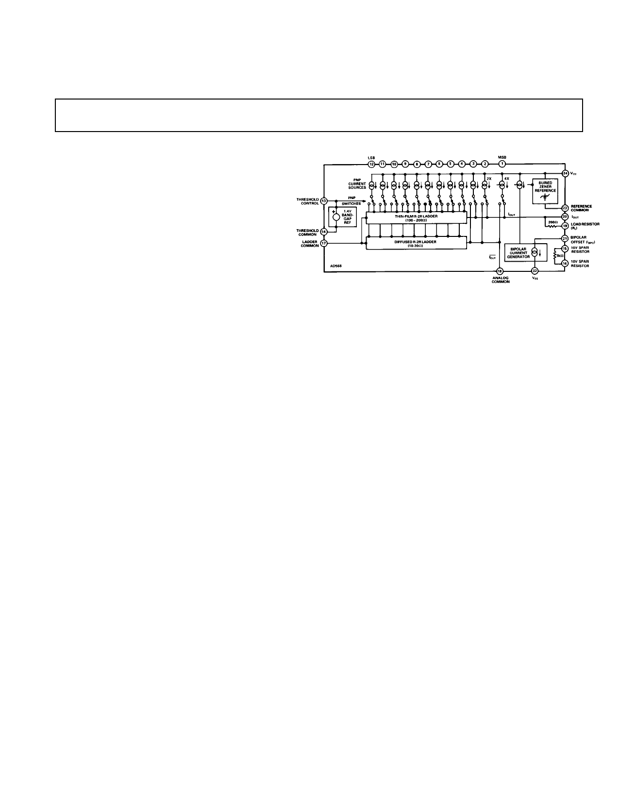
FUNCTIONAL BLOCK DIAGRAM
PRODUCT DESCRIPTION
The AD568 is an ultrahigh-speed, 12-bit digital-to-analog con-
verter (DAC) settling to 0.025% in 35 ns. The monolithic de-
vice is fabricated using Analog Devices’ Complementary Bipolar
(CB) Process. This is a proprietary process featuring high-speed
NPN and PNP devices on the same chip without the use of di-
electric isolation or multichip hybrid techniques. The high speed
of the AD568 is maintained by keeping impedance levels low
enough to minimize the effects of parasitic circuit capacitances.
The DAC consists of 16 current sources configured to deliver a
10.24 mA full-scale current. Multiple matched current sources
and thin-film ladder techniques are combined to produce bit
weighting. The DAC’s output is a 10.24 mA full scale (FS) for
current output applications or a 1.024 V FS unbuffered voltage
output. Additionally, a 10.24 V FS buffered output may be gen-
erated using an onboard 1 kΩ span resistor with an external op
amp. Bipolar ranges are accomplished by pin strapping.
Laser wafer trimming insures full 12-bit linearity. All grades of
the AD568 are guaranteed monotonic over their full operating
temperature range. Furthermore, the output resistance of the
DAC is trimmed to 100 Ω ± 1.0%. The gain temperature coeffi-
cient of the voltage output is 30 ppm/°C max (K).
The AD568 is available in three performance grades. The
AD568JQ and KQ are available in 24-pin cerdip (0.3") packages
and are specified for operation from 0°C to +70°C. The
AD568SQ features operation from –55°C to +125°C and is also
packaged in the hermetic 0.3" cerdip.
PRODUCT HIGHLIGHTS
1. The ultrafast settling time of the AD568 allows leading edge
performance in waveform generation, graphics display and
high speed A/D conversion applications.
2. Pin strapping provides a variety of voltage and current output
ranges for application versatility. Tight control of the abso-
lute output current reduces trim requirements in externally-
scaled applications.
3. Matched on-chip resistors can be used for precision scaling in
high speed A/D conversion circuits.
4. The digital inputs are compatible with TTL and +5 V
CMOS logic families.
5. Skinny DIP (0.3") packaging minimizes board space require-
ments and eases layout considerations.
6. The AD568 is available in versions compliant with MIL-
STD-883. Refer to the Analog Devices Military Products
Databook or current AD568/883B data sheet for detailed
specifications.
REV. A
Information furnished by Analog Devices is believed to be accurate and
reliable. However, no responsibility is assumed by Analog Devices for its
use, nor for any infringements of patents or other rights of third parties
which may result from its use. No license is granted by implication or
otherwise under any patent or patent rights of Analog Devices.
One Technology Way, P.O. Box 9106, Norwood, MA 02062-9106, U.S.A.
Tel: 617/329-4700
Fax: 617/326-8703
1 page 
AD568
+15V
–15V
0.2µF
DIGITAL
INPUTS
1 +15V 24
0.1µF
2 REFCOM 23
3 –15V 22 0.1µF
4 IBPO 21
5 IOUT 20
6 AD568 RL 19
7 ACOM 18
8 LCOM 17
9 SPAN 16 NC
10 SPAN 15 NC
11 THCOM 14
100pF
12 VTH 13
RTH
1kΩ
0.1µF
ANALOG
OUTPUT
ANALOG
GND PLANE
DIGITAL
GND PLANE
ANALOG
SUPPLY
GROUND
DIGITAL
SUPPLY
GROUND
full scale at the DAC output. Note: this may slightly compro-
mise the bipolar zero trim.
DIGITAL
INPUTS
1 BIT 1
2 MSB
24
23
3 AD568 22
4 IBPO 21
5 IOUT 20
6 RL 19
7 ACOM 18
8 LCOM 17
9 16
10 15
11
12
BIT 12
LSB
14
13
GAIN
20Ω
VCC
5.11kΩ
75Ω
ZERO
20kΩ
ANALOG
OUTPUT
(–0.512 TO
0.512V)
VEE
Figure 7. Bipolar Unbuffered Gain and Zero Adjust
+5V
Figure 5. Bipolar Output Unbuffered ±1.024 V
Optional Gan and Zero Adjustment
The gain and offset are laser trimmed to minimize their effects
on circuit performance. However, in some applications, it may
be desirable to externally reduce these errors further. In those
cases, the following procedures are suggested.
UNIPOLAR MODE: (Refer to Figure 6)
Step 1 – Set all bits (BIT 1–BIT 12) to Logic “0” (OFF)—note
the output voltage. This is the offset error.
Step 2 – Set all bits to Logic “1” (ON). Adjust the gain trim re-
sistor so that the output voltage is equal to the desired full scale
minus 1 LSB plus the offset error measured in step 1.
Step 3 – Reset all bits to Logic “0” (OFF). Adjust the offset
trim resistor for 0 V output.
DIGITAL
INPUTS
1 BIT 1
2 MSB
24
23
3 AD568 22
4 IBPO 21
5 IOUT 20
6 RL 19
7 ACOM 18
8 LCOM 17
9 16
10 15
11
12
BIT 12
LSB
14
13
GAIN
20Ω
5.11kΩ
100Ω
OFFSET
ANALOG
OUTPUT
(0 TO 1.024V)
Figure 6. Unbuffered Unipolar Gain and Zero Adjust
BIPOLAR MODE (Refer to Figure 7)
Step 1 – Set bits to offset binary “zero” (10 . . . 00). Adjust the
zero resistor to produce 0 V at the DAC output. This removes
the bipolar zero error.
Step 2 – Set all bits to Logic “1” (ON). Adjust gain trim resistor
so the output voltage is equal to the desired full-scale minus
l LSB .
Step 3 – (Optional) If precise trimming of the bipolar offset is
preferred to trimming of bipolar zero: set all bits to Logic “0”
(OFF). Trim the zero resistor to produce the desired negative
BUFFERED VOLTAGE OUTPUT
For full-scale outputs of greater than 1 V, some type of external
buffer amplifier is required. The AD840 fills this requirement
perfectly, settling to 0.025% from a 10 V full-scale step in less
than 100 ns.
A 1 kΩ span resistor has been provided on chip for use as a
feedback resistor in buffered applications. Using RSPAN (Pins 15,
16) introduces a 100 mW code-dependent power source onto
the chip which may generate a slight degradation in linearity.
Maximum linearity performance can be realized by using an ex-
ternal span resistor.
+15V –15V
0.2µF
0.1µF
DIGITAL
INPUTS
1 +15V 24
0.1µF
2 REFCOM 23
0.1µF
3 –15V 22
4 IBPO 21
5 IOUT 20
6 AD568 RL 19
7 ACOM 18
8 LCOM 17
9 SPAN 16
5pF
10 SPAN 15
11 THCOM 14
100pF
12 VTH 13
RTH
1kΩ
–VS
100Ω
+VS
AD840
ANALOG
OUTPUT
ANALOG
GND PLANE
ANALOG
SUPPLY
GROUND
DIGITAL
GND PLANE
DIGITAL
SUPPLY
GROUND
AMPLIFIER NOISE GAIN: 11
+5V
Figure 8. Unipolar Output Buffered 0 to –10.24V
Unipolar Inverting Configuration
Figure 8 shows the connections for producing a – 10.24 V full-
scale swing. This configuration uses the AD568 in the current
output mode into a summing junction at the inverting input ter-
minal of the external op amp. With the load resistor RL
grounded, the DAC has an output impedance of 100 Ω. This
produces a noise gain of 11 from the noninverting terminal of
the op amp, and hence, satisfies the stability criterion of the
AD840 (stable at a gain of 10). The addition of a 5 pF compen-
REV. A
–5–
5 Page 
DIGITAL GROUND CLOCK
PLANE
INPUT
WORDS
5V
ANALOG GROUND
PLANE
+15V
–15V
OUTPUT
5V
AD568
SETTLING/GLITCH
EVALUATION BOARD
AD568
High-Speed Interconnect and Routing
It is essential that care be taken in the signal and power ground
circuits to avoid inducing extraneous voltage drops in the signal
ground paths. It is suggested that all connections be short and
direct, and as physically close to the package as possible, so that
the length of any conduction path shared by external compo-
nents will be minimized. When runs exceed an inch or so in
length, some type of termination resistor may be required. The
necessity and value of this resistor will be dependent upon the
logic family used.
For maximum ac performance, the DAC should be mounted di-
rectly to the circuit board; sockets should not be used as they in-
troduce unwanted capacitive coupling between adjacent pins of
the device.
Component Side
ANALOG VCC
ANALOG VEE
ANALOG +5V
+5V
Applications
1 s, 12-BIT SUCCESSIVE APPROXIMATION A/D
CONVERTER
The AD568’s unique combination of high speed and true 12-bit
accuracy can be used to construct a 12-bit SAR-type A/D con-
verter with a sub-µs conversion time. Figure 19 shows the con-
figuration used for this application. A negative analog input
voltage is converted into current and brought into a summing
junction with the DAC current. This summing junction is
bidirectionally clamped with two Schottky diodes to limit its
voltage excursion from ground. This voltage is differentially am-
plified and passed to a high-speed comparator. The comparator
output is latched and fed back to the successive approximation
register, which is then clocked to generated the next set of codes
for the DAC.
Foil Side
Figure 18. Printed Circuit Board Layout
+15V
VI N
–15V 0 TO –10.24V
0.2µF
+5V –5V
2.5k –5V
COMPARATOR
LT1016
+5V
24 VCC
12 GND
Q11 21
Q10 20
2 D0 SAR Q9 19
23 Q11 2504 Q8 18
10 NC
Q7 17
15 NC
Q6 16
22 NC
Q5 9
13 CP
Q4 8
1E
14 S
3 CC
11 D
Q3 7
Q2 6
Q1 5
Q0 4
1 +15V 24
0.1µF
2 REFCOM 23
0.1µF
3 –15V 22
4 IBPO 21
5 DAC IOUT 20
6 AD568 RL 19
7 ACOM 18
8 LCOM 17
9 SPAN 16 NC
10 SPAN 15 NC
11
THCOM 14
100pF
12 VTH 13
1k
0.1µF
1k
0.01µF
620 620
150
Q3
1k
D3
IN4148
Q1 Q2
1 V+
2 +IN
3 –IN
4 V–
OUT 8
OUT 7
GND 6
LCH 5
D1
ANALOG
GND PLANE
+5V
D2
27k
–15V
15kΩ
Q4
150kΩ
INVERTER
74HC04
PARALLEL DATA
OUT
150kΩ
Q5
CONVERSION COMPLETE
START COMVERT
CHIP ENABLE
+5V
REV. A
Figure 19. AD568 1 µs Successive Approximation A/D Application
–11–
11 Page | ||
| Páginas | Total 14 Páginas | |
| PDF Descargar | [ Datasheet AD568.PDF ] | |
Hoja de datos destacado
| Número de pieza | Descripción | Fabricantes |
| AD5601 | (AD5601 - AD5621) SPI Interface / SC70 Package / nanoDAC D/A | Analog Devices |
| AD5602 | 8-/10-/12-Bit nanoDACs | Analog Devices |
| AD561 | Low Cost 10-Bit Monolithic D/A Converter | Analog Devices |
| AD5611 | (AD5601 - AD5621) SPI Interface / SC70 Package / nanoDAC D/A | Analog Devices |
| Número de pieza | Descripción | Fabricantes |
| SLA6805M | High Voltage 3 phase Motor Driver IC. |
Sanken |
| SDC1742 | 12- and 14-Bit Hybrid Synchro / Resolver-to-Digital Converters. |
Analog Devices |
|
DataSheet.es es una pagina web que funciona como un repositorio de manuales o hoja de datos de muchos de los productos más populares, |
| DataSheet.es | 2020 | Privacy Policy | Contacto | Buscar |