|
|
PDF AD1385 Data sheet ( Hoja de datos )
| Número de pieza | AD1385 | |
| Descripción | 16-Bit 500 kHz Wide Temperature Range Sampling ADC | |
| Fabricantes | Analog Devices | |
| Logotipo |  |
|
Hay una vista previa y un enlace de descarga de AD1385 (archivo pdf) en la parte inferior de esta página. Total 20 Páginas | ||
|
No Preview Available !
a
FEATURES
16-Bit Resolution
500 kHz Sampling Rate
Differential Linearity Autocalibration
Specified over –55؇C to +125؇C Range
SNR 90 dB @ 100 kHz (min)
THD –88 dB @ 100 kHz (min)
0.0006% FSR DNL (typ)
0.0015% FSR INL (typ)
No Missing Codes
؎5, ؎10 V Bipolar Input Ranges
Zero Offset Autocalibration
APPLICATIONS
Medical Imaging
CAT
Magnetic Resonance
Radar
Vibration Analysis
Parametric Measurement Unit (ATE)
Digital Storage Oscilloscopes
Waveform Recorders
Analytical Instruments
16-Bit 500 kHz
Wide Temperature Range Sampling ADC
AD1385
FUNCTIONAL BLOCK DIAGRAM
PRODUCT DESCRIPTION
The AD1385 is a complete 500 kHz, 16-bit, sampling analog-
to-digital converter contained in a single package. Its differential
linearity autocalibration feature allows this high resolution, high
speed converter to offer outstanding noise and distortion perfor-
mance, as well as excellent INL and DNL specifications, over
the full military temperature range. Autocalibration effectively
eliminates DNL drift over temperature.
The AD1385 architecture includes a low noise, low distortion
track/hold, a three pass digitally corrected subranging ADC, and
linearity calibration circuitry. A complete linearity calibration
requires only 15 ms. Precision thin-film resistors and a propri-
etary DAC contribute to the part’s outstanding dynamic and
static performance.
The AD1385 uses four power supplies, ± 5 V and ± 15 V, and an
external 10 MHz clock. Power dissipation is nominally 2.76 W.
Two user selectable bipolar input ranges, ± 5 V and ± 10 V, are
provided. Careful attention to grounding and a single package
make it easy to design PCBs to achieve specified performance.
The AD1385’s pinout is nearly identical to that of the AD1382,
a factory calibrated 16-bit, 500 kHz SADC. Just two additional
connections, to enable and monitor autocalibration, are required.
This commonality provides an easy upgrade path to extend sys-
tem performance and operating temperature range.
REV. 0
Information furnished by Analog Devices is believed to be accurate and
reliable. However, no responsibility is assumed by Analog Devices for its
use, nor for any infringements of patents or other rights of third parties
which may result from its use. No license is granted by implication or
otherwise under any patent or patent rights of Analog Devices.
One Technology Way, P.O. Box 9106, Norwood, MA 02062-9106, U.S.A.
Tel: 617/329-4700
Fax: 617/326-8703
1 page 
AD1385
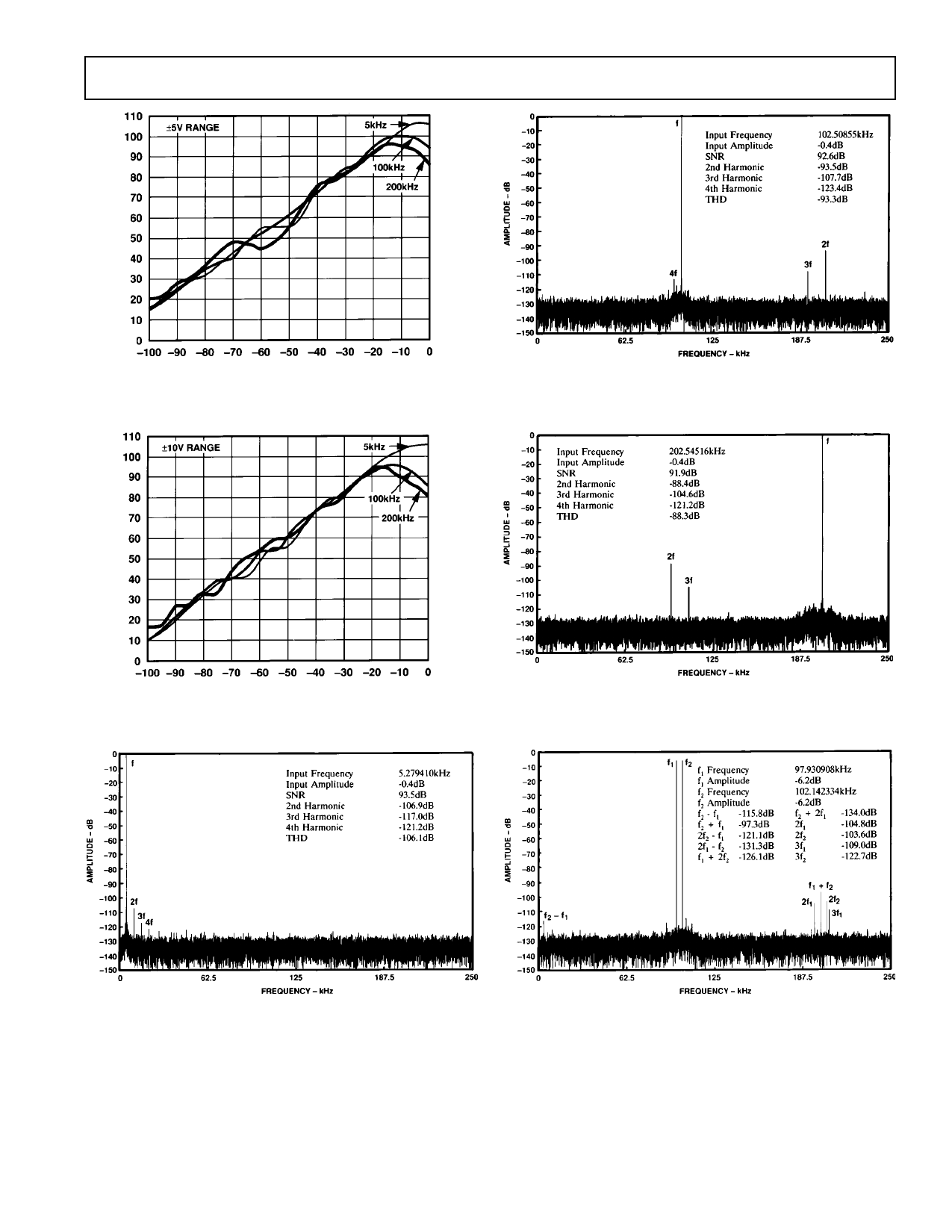
Figure 1. Spurious-Free Range vs. Input Amplitude,
±5 V Range, 2048-Point FFT, 500 kHz Sample Rate
Figure 4. Full-Scale Sine Wave Power Spectral Density,
±5 V Range, 16384-Point FFT, 500 kHz Sample Rate
Figure 2. Spurious-Free Range vs. Input Amplitude,
±10 V Range, 2048-Point FFT, 500 kHz Sample Rate
Figure 5. Full-Scale Sine Wave Power Spectral Density,
±5 V Range, 16384-Point FFT, 500 kHz Sample Rate
Figure 3. Full-Scale Sine Wave Power Spectral Density,
±5 V Range, 16384-Point FFT, 500 kHz Sample Rate
Figure 6. 100 kHz Intermodulation Performance, ±5 V
Range, 16384-Point FFT, 500 kHz Sample Rate
REV. 0
–5–
5 Page 
AD1385
mode as long either Hold Command Out or Start Convert is
high. Care is needed in defining system timing to ensure that
the T/H has a minimum of 700 ns for signal acquisition before
another conversion begins. The minimum width of Start Con-
vert is 20 ns, the sum of tSCS and tSCH, the minimum setup and
hold times.
Transmission line effects at the Start Convert and Hold Com-
mand In inputs should be considered when designing circuit
boards for the AD1385. A series termination resistor of 50 Ω to
100 Ω is recommended when the source of either of these sig-
nals is more than a few inches away from the AD1385. This will
control reflections and transients which could otherwise degrade
the part’s performance.
Output Data
The output data are multiplexed in two bytes onto an 8-bit data
bus. Data are guaranteed to be stable at the time of the edges of
Data Strobe (Pin 15). Hi/Lo Byte Select (Pin 16) controls
which byte is presented first. If Hi/Lo Byte Select is high, then
BYTE0 is B9–B16 and BYTE1 is B1–B8. The order of the data
bytes is interchanged when Hi/Lo Byte Select is low. BYTE 0
and BYTE 1 are defined in the timing diagram Figure 17. B1 is
the most significant bit of the reconstructed 16-bit data.
B1 SELECT (Pin 44) determines whether data is presented in
complementary twos complement or complementary offset bi-
nary form. Complementary twos complement data is provided
when B1 Select is LOW. OE may be used to place the data bus
into a high impedance state.
The arithmetic unit in the AD1385 saturates at all 0s or all 1s if
the input range is exceeded.
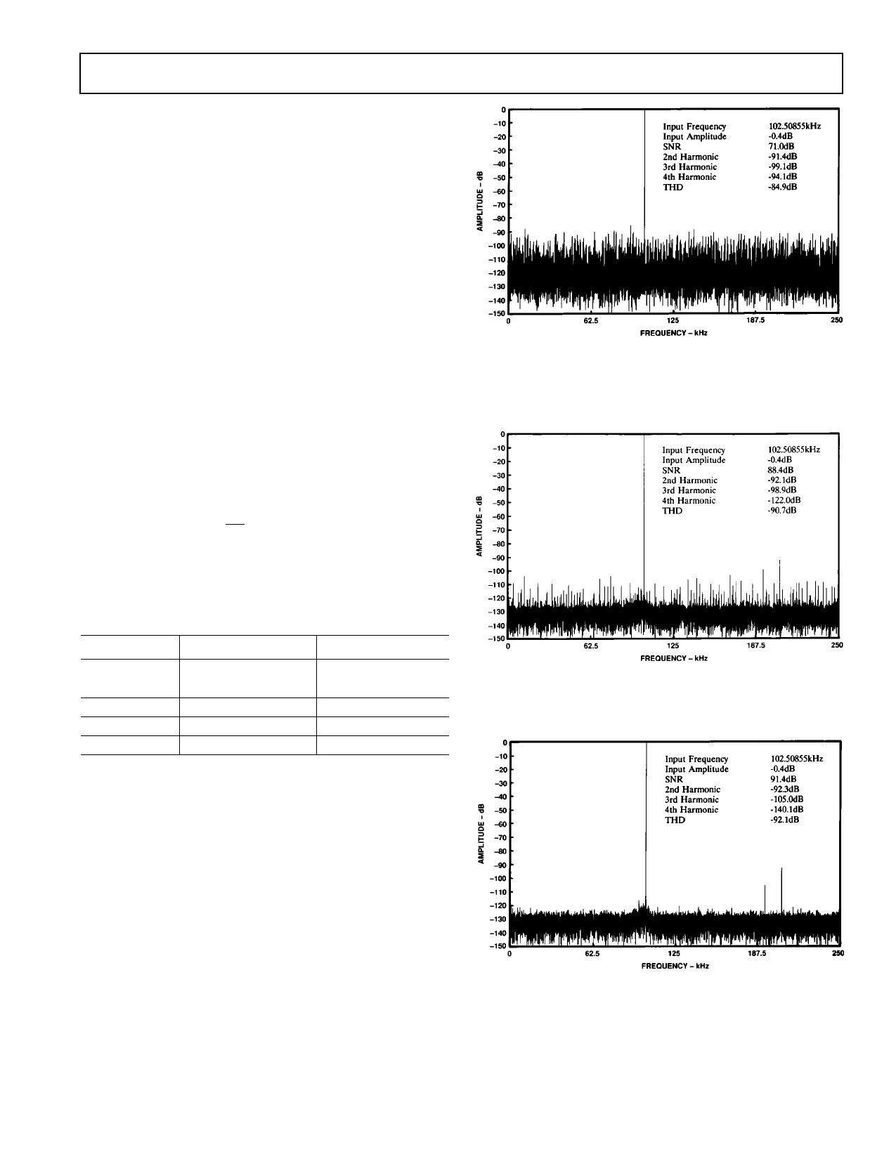
Figure 20. Full-Scale Power Spectral Density after Power-
up at TCASE = +25°C Without Calibration, ±5 V Range,
16384-Point FFT, 500 kHz Sample Rate. Compare with
Figure 4.
Table I.
B1 Select
0
1
Data Format
–Full-Scale Data
0 V Data
+Full-Scale Data
Complementary Twos Complementary Offset
Complement
Binary
7FFFH
FFFFH
FFFFH
8000H
8000H
0000H
Figure 21. Full-Scale Power Spectral Density at TCASE =
+125°C, Calibration Performed at TCASE = +25°C, ±5 V
Range, 16384-Point FFT, 500 kHz Sample Rate
CALIBRATION (Pins 28 and 41)
Calibration corrects for linearity errors in the Reference DAC
arising from internal component mismatches or temperature
changes. It has a negligible effect on gain and offset errors, and
these should be corrected by other means. The AD1385 must
be calibrated after power-up, and recalibration is recommended
whenever the part’s temperature has changed by more than
15°C. Performance degrades gracefully with temperature
changes, resulting in small but gradual decreases in SNR and
increases in distortion which may be eliminated by recalibra-
tion. Calibration codes are stored in internal RAM and are lost
when power is removed. Figures 20–22 show the effects of
uncalibrated versus calibrated operation.
Figure 22. Same as Figure 21 Following Recalibration at
TCASE = +125°C
REV. 0
–11–
11 Page | ||
| Páginas | Total 20 Páginas | |
| PDF Descargar | [ Datasheet AD1385.PDF ] | |
Hoja de datos destacado
| Número de pieza | Descripción | Fabricantes |
| AD1380 | Low Cost 16-Bit Sampling ADC | Analog Devices |
| AD1382 | 16-Bit 500 kHz Sampling ADC | Analog Devices |
| AD1385 | 16-Bit 500 kHz Wide Temperature Range Sampling ADC | Analog Devices |
| Número de pieza | Descripción | Fabricantes |
| SLA6805M | High Voltage 3 phase Motor Driver IC. |
Sanken |
| SDC1742 | 12- and 14-Bit Hybrid Synchro / Resolver-to-Digital Converters. |
Analog Devices |
|
DataSheet.es es una pagina web que funciona como un repositorio de manuales o hoja de datos de muchos de los productos más populares, |
| DataSheet.es | 2020 | Privacy Policy | Contacto | Buscar |
