|
|
|
PDF AD1671 Data sheet ( Hoja de datos )
| Número de pieza | AD1671 | |
| Descripción | Complete 12-Bit 1.25 MSPS Monolithic A/D Converter | |
| Fabricantes | Analog Devices | |
| Logotipo | ||
Hay una vista previa y un enlace de descarga de AD1671 (archivo pdf) en la parte inferior de esta página. Total 16 Páginas | ||
|
No Preview Available !
a
Complete 12-Bit 1.25 MSPS
Monolithic A/D Converter
AD1671
FEATURES
Conversion Time: 800 ns
1.25 MHz Throughput Rate
Complete: On-Chip Sample-and-Hold Amplifier and
Voltage Reference
Low Power Dissipation: 570 mW
No Missing Codes Guaranteed
Signal-to-Noise Plus Distortion Ratio
fIN = 100 kHz: 70 dB
Pin Configurable Input Voltage Ranges
Twos Complement or Offset Binary Output Data
28-Pin DIP and 28-Pin Surface Mount Package
Out of Range Indicator
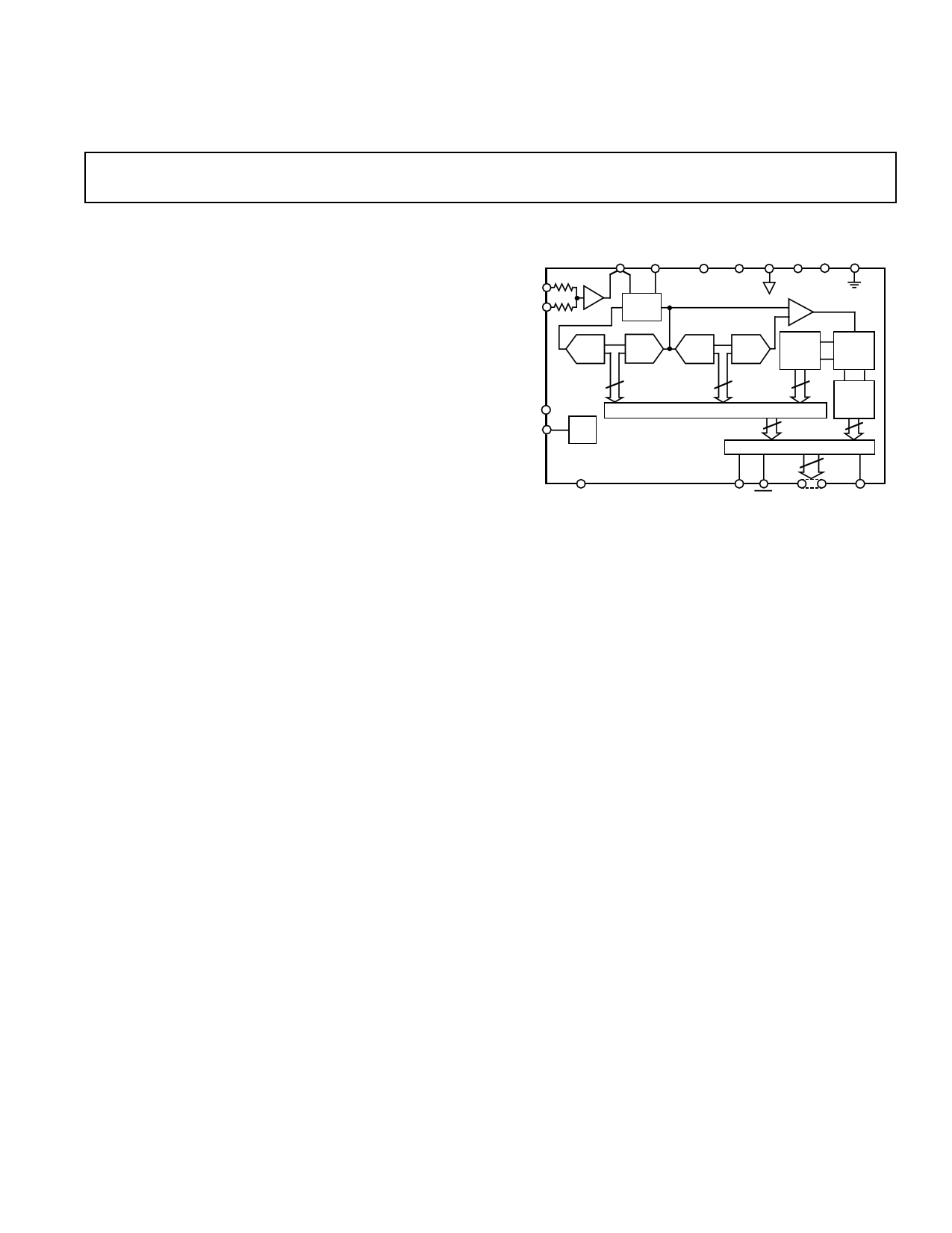
FUNCTIONAL BLOCK DIAGRAM
AIN1
AIN2
SHA
OUT UPO/BPO ENCODE VCC ACOM VEE VLOGIC DCOM
5k
S/H
RANGE
5k SELECT
X4
3-BIT
FLASH
DAC
3-BIT
FLASH
DAC
COARSE
4-BIT
FLASH
8-BIT
LADDER
MATRIX
REF IN
REF OUT
3 3 4 FINE
4-BIT
CORRECTION LOGIC
FLASH
2.5V
REF
AD1671
8
LATCHES
12
4
PRODUCT DESCRIPTION
The AD1671 is a monolithic 12-bit, 1.25 MSPS analog-to-
digital converter with an on-board, high performance sample-
and-hold amplifier (SHA) and voltage reference. The AD1671
guarantees no missing codes over the full operating tempera-
ture range. The combination of a merged high speed bipolar/
CMOS process and a novel architecture results in a combi-
nation of speed and power consumption far superior to pre-
viously available hybrid implementations. Additionally, the
greater reliability of monolithic construction offers improved
system reliability and lower costs than hybrid designs.
The fast settling input SHA is equally suited for both multi-
plexed systems that switch negative to positive full-scale
voltage levels in successive channels and sampling inputs at
frequencies up to and beyond the Nyquist rate. The AD1671
provides both reference output and reference input pins, al-
lowing the on-board reference to serve as a system reference.
An external reference can also be chosen to suit the dc accu-
racy and temperature drift requirements of the application.
The AD1671 uses a subranging flash conversion technique,
with digital error correction for possible errors introduced in
the first part of the conversion cycle. An on-chip timing gen-
erator provides strobe pulses for each of the four internal
flash cycles. A single ENCODE pulse is used to control the
converter. The digital output data is presented in twos
complement or offset binary output format. An out-of-range
signal indicates an overflow condition. It can be used with
the most significant bit to determine low or high overflow.
REF COM
OTR MSB
BIT 1 –12
DAV
The performance of the AD1671 is made possible by using high
speed, low noise bipolar circuitry in the linear sections and low
power CMOS for the logic sections. Analog Devices’ ABCMOS-1
process provides both high speed bipolar and 2-micron CMOS
devices on a single chip. Laser trimmed thin-film resistors are
used to provide accuracy and temperature stability.
The AD1671 is available in two performance grades and three
temperature ranges. The AD1671J and K grades are available
over the 0°C to +70°C temperature range. The AD1671A grade
is available over the –40°C to +85°C temperature range. The
AD1671S grade is available over the –55°C to +125°C tempera-
ture range.
PRODUCT HIGHLIGHTS
The AD1671 offers a complete single chip sampling 12-bit,
1.25 MSPS analog-to-digital conversion function in a 28-pin
package.
The AD1671 at 570 mW consumes a fraction of the power of
currently available hybrids.
An OUT OF RANGE output bit indicates when the input sig-
nal is beyond the AD1671’s input range.
Input signal ranges are 0 V to +5 V unipolar or ± 5 V bipolar,
selected by pin strapping, with an input resistance of 10 kΩ.
The input signal range can also be pin strapped for 0 V to +2.5 V
unipolar or ±2.5 V bipolar with an input resistance of 10 MΩ.
Output data is available in unipolar, bipolar offset or bipolar
twos complement binary format.
REV. B
Information furnished by Analog Devices is believed to be accurate and
reliable. However, no responsibility is assumed by Analog Devices for its
use, nor for any infringements of patents or other rights of third parties
which may result from its use. No license is granted by implication or
otherwise under any patent or patent rights of Analog Devices.
One Technology Way, P.O. Box 9106, Norwood, MA 02062-9106, U.S.A.
Tel: 617/329-4700
Fax: 617/326-8703
1 page 
ABSOLUTE MAXIMUM RATINGS*
Parameter With Respect to Min
Max
Units
VCC
VEE
VLOGIC
ACOM
ACOM
ACOM
DCOM
DCOM
VCC
VLOGIC
ENCODE DCOM
REF IN ACOM
AIN ACOM
BPO/UPO ACOM
Junction Temperature
Storage Temperature
Lead Temperature (10 sec)
–0 5
–6.5
–0.5
–1.0
–6.5
–0.5
–0.5
–11.0
–0.5
–65
+6.5 Volts
+0.5 Volts
+6.5 Volts
+1.0 Volts
+6.5 Volts
VLOGIC + 0.5 Volts
VCC + 0.5 Volts
+11.0
Volts
VCC + 0.5 Volts
+150
°C
+150
°C
+300
°C
*Stresses above those listed under “Absolute Maximum Ratings” may cause
permanent damage to the device. This is a stress rating only and functional
operation of the device at these or any other conditions above those indicated in
the operational sections of this specification is not implied. Exposure to absolute
maximum ratings for extended periods may effect device reliability.
AD1671
ORDERING GUIDE
Model1
AD1671JQ
AD1671KQ
AD1671JP
AD1671KP
AD1671AQ
AD1671AP
AD1671SQ
Linearity
± 2.5 LSB
± 2 LSB
± 2.5 LSB
± 2 LSB
± 2.5 LSB
± 2.5 LSB
± 3 LSB
Temperature
Range
0°C to +70°C
0°C to +70°C
0°C to +70°C
0°C to +70°C
–40°C to +85°C
–40°C to +85°C
–55°C to +125°C
Package
Option2, 3
Q-28
Q-28
P-28A
P-28A
Q-28
P-28A
Q-28
NOTES
1For details on grade and package offerings screened in accordance with
MIL-STD-883, refer to Analog Devices’ Military Products Databook or
current AD1671/883 data sheet.
2P = Plastic Leaded Chip Carrier, Q = Cerdip.
3Analog Devices reserves the right to ship side brazed ceramic packages in
lieu of cerdip.
CAUTION
ESD (electrostatic discharge) sensitive device. Electrostatic charges as high as 4000 V readily
accumulate on the human body and test equipment and can discharge without detection.
Although the AD1671 features proprietary ESD protection circuitry, permanent damage may
occur on devices subjected to high energy electrostatic discharges. Therefore, proper ESD
precautions are recommended to avoid performance degradation or loss of functionality.
WARNING!
ESD SENSITIVE DEVICE
REV. B
–5–
5 Page 
AD1671
Table III. Output Data Format
Input
Range
Coding
Analog
Inputl
Digital
Output
0 V to +2.5 V Straight Binary
≤ –0.0003 V
0V
+2.5 V
≥ +2.5003 V
0 V to +5 V
Straight Binary
≤ –0.0006 V
0V
+5 V
≥ +5.0006 V
–2.5 V to +2.5 V Offset Binary
≤ –2.5006 V
–2.5 V
+2.5 V
≥ +2.4994 V
–5 V to +5 V Offset Binary
≤ –5.0012 V
–5 V
+5 V
≥ +4.9988 V
–2.5 V to +2.5 V
Twos Complement
(Using MSB)
≤ –2.5006 V
–2.5 V
+2.5 V
≥ +2.4994 V
–5 V to +5 V
Twos Complement
(Using MSB)
≤ –5.0012 V
–5 V
+5 V
≥ +4.9988 V
0000 0000 0000
0000 0000 0000
1111 1111 1111
1111 1111 1111
0000 0000 0000
0000 0000 0000
1111 1111 1111
1111 1111 1111
0000 0000 0000
0000 0000 0000
1111 1111 1111
1111 1111 1111
0000 0000 0000
0000 0000 0000
1111 1111 1111
1111 1111 1111
1000 0000 0000
1000 0000 0000
0111 1111 1111
0111 1111 1111
1000 0000 0000
1000 0000 0000
0111 1111 1111
0111 1111 1111
NOTES
1Voltages listed are with offset and gain errors adjusted to zero.
2Typical performance.
OTR2
1
0
0
1
1
0
0
1
1
0
0
1
1
0
0
1
1
0
0
1
1
0
0
1
OUTPUT DATA FORMAT
The AD1671 provides both MSB and MSB outputs, delivering
data in positive true straight binary for unipolar input ranges
and positive true offset binary or twos complement for bipolar
input ranges. Straight binary coding is used for systems that ac-
cept positive-only signals. If straight binary coding is used with
bipolar input signals, a 0 V input would result in a binary output
of 2048. The application software would have to subtract 2048
to determine the true input voltage. Host registers typically per-
form math on signed integers and assume data is in that format.
Twos complement format minimizes software overhead which is
especially important in high speed data transfers, such as a
DMA operation. The CPU is not bogged down performing data
conversion steps, hence the total system throughput is increased.
OPTIONAL EXTERNAL REFERENCE
The AD1671 includes an onboard +2.5 V reference. The refer-
ence input pin (REF IN) can be connected to reference output
pin (REF OUT) or a standard external +2.5 V reference can be
selected to meet specific system requirements. Fast switching in-
put dependent currents are modulated at the reference input.
The reference input voltage can be held with the use of a capaci-
tor. To prevent the AD1671’s onboard reference from oscil-
lating when not connected to REF IN, REF OUT must be
connected to +5 V. It is possible to connect REF OUT to +5 V
due to its output circuit implementation which shuts down the
reference.
ILOGIC VS. CONVERSION RATE
Figure 15 is the typical logic supply current vs. conversion rate
for various capacitor loads on the digital outputs.
6.5
6.0
5.5
5.0
4.5
4.0
3.5 CL = 50pF
3.0
2.5
2.0 CL = 30pF
1.5
1.0
0.5
1k
10k 100k
CONVERSION RATE – Hz
CL = 0pF
1M
Figure 15. ILOGIC vs. Conversion Rate for Various
Capacitive Loads on the Digital Outputs
REV. B
–11–
11 Page | ||
| Páginas | Total 16 Páginas | |
| PDF Descargar | [ Datasheet AD1671.PDF ] | |
Hoja de datos destacado
| Número de pieza | Descripción | Fabricantes |
| AD1671 | Complete 12-Bit 1.25 MSPS Monolithic A/D Converter | Analog Devices |
| AD1672 | Complete 12-Bit/ 3 MSPS Monolithic A/D Converter | Analog Devices |
| AD1674 | 12-Bit 100 kSPS A/D Converter | Analog Devices |
| Número de pieza | Descripción | Fabricantes |
| SLA6805M | High Voltage 3 phase Motor Driver IC. |
Sanken |
| SDC1742 | 12- and 14-Bit Hybrid Synchro / Resolver-to-Digital Converters. |
Analog Devices |
|
DataSheet.es es una pagina web que funciona como un repositorio de manuales o hoja de datos de muchos de los productos más populares, |
| DataSheet.es | 2020 | Privacy Policy | Contacto | Buscar |