|
|
|
PDF AD2S99 Data sheet ( Hoja de datos )
| Número de pieza | AD2S99 | |
| Descripción | Programmable Oscillator | |
| Fabricantes | Analog Devices | |
| Logotipo | ||
Hay una vista previa y un enlace de descarga de AD2S99 (archivo pdf) en la parte inferior de esta página. Total 8 Páginas | ||
|
No Preview Available !
a
FEATURES
Programmable Sinusoidal Oscillator
Synthesized Synchronous Reference Output
Programmable Output Frequency Range: 2 kHz–20 kHz
“Loss-of-Signal” Indicator
20-Pin PLCC Package
Low Cost
APPLICATIONS
Excitation Source for:
Resolvers
Synchros
LVDTs
RVDTs
Pressure Transducers
Load Cells
AC Bridges
Programmable
Oscillator
AD2S99
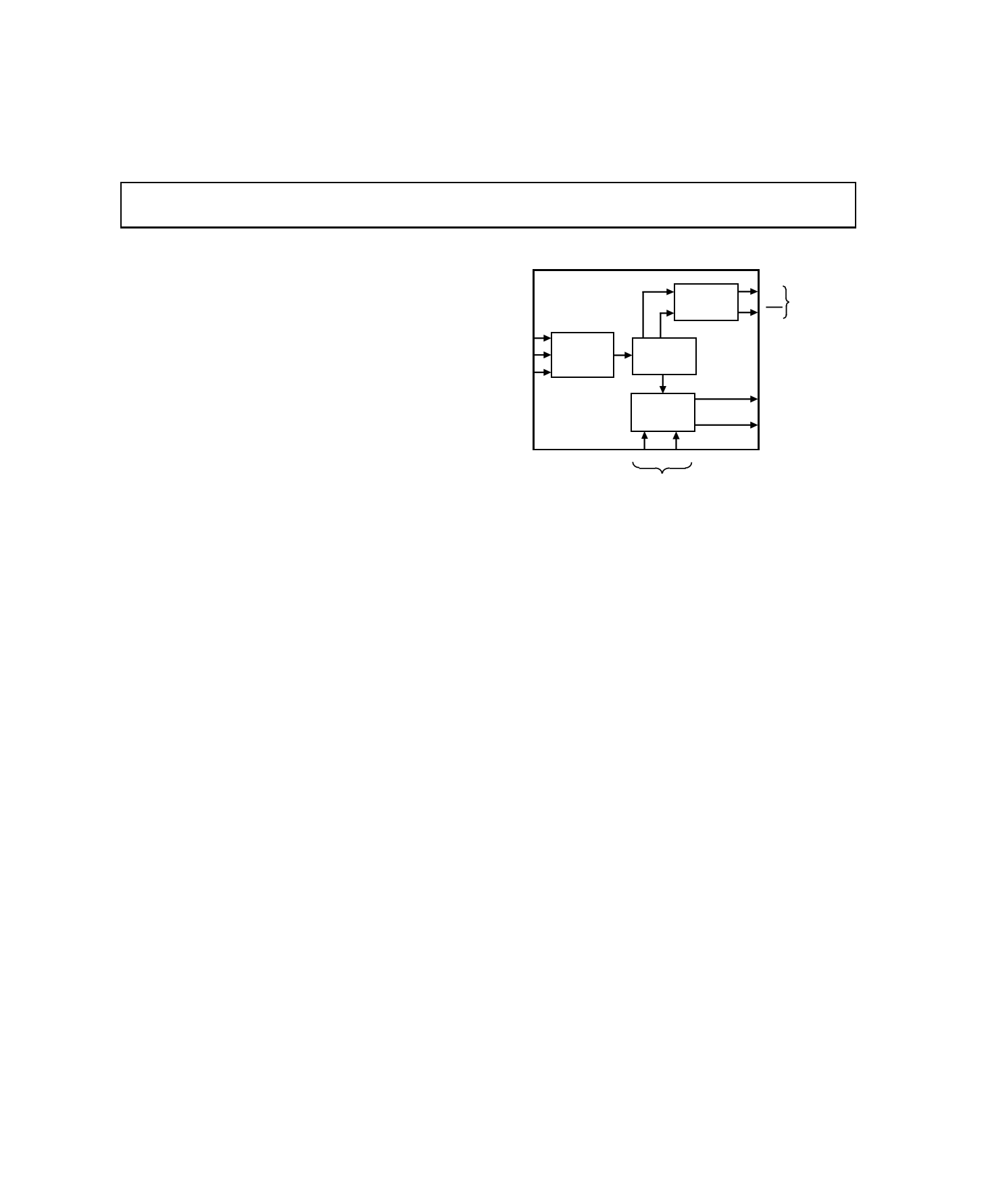
FUNCTIONAL BLOCK DIAGRAM
FBIAS
SEL1
SEL2
FREQUENCY
SELECT
PUSH/
PULL
O/P STAGE
SINE WAVE
GENERATOR
AD2S99
PHASE
DETECT
LOGIC
SIN COS
FROM
TRANSDUCER
EXC TO
TRANSDUCER
EXC
SYNREF
SYNCHRONOUS
REFERENCE
LOS
GENERAL DESCRIPTION
The AD2S99 programmable sinusoidal oscillator provides sine
wave excitation for resolvers and a wide variety of ac transduc-
ers. The AD2S99 also provides a synchronous reference output
signal (3 V p-p square wave) that is phase locked to its SIN and
COS inputs. In an application, the SIN and COS inputs are
connected to the transducer’s secondary windings.
The synchronous reference output compensates for temperature
and cabling dependent phase shifts and eliminates the need for
external preset phase compensation circuits. The synchronous
reference output can be used as a zero crossing reference for
resolver-to-digital converters such as Analog Devices’ AD2S80A,
AD2S82A, AD2S83 and AD2S90.
The AD2S99 is packaged in a 20-pin PLCC and operates over
–40°C to +85°C.
PRODUCT HIGHLIGHTS
Dynamic Phase Compensation
The AD2S99 dynamically compensates for any phase variation
in a transducer by phase locking its synchronous reference out-
put to the transducer’s secondary windings.
Programmable Excitation Frequency
The excitation frequency is easily programmed to 2 kHz, 5 kHz,
10 kHz, or 20 kHz by using the frequency select pins. Interme-
diate frequencies are available by adding an external resistor.
Signal Loss Detection
The AD2S99 has the ability to detect if both the transducer sec-
ondary winding connections become disconnected from its SIN
and COS inputs. The “LOS” output pin pulls high when a sig-
nal loss is detected.
Integration
The AD2S99 integrates the transducer excitation, synchronous
reference, and loss of signal detection functions into a small,
cost effective package.
REV. B
Information furnished by Analog Devices is believed to be accurate and
reliable. However, no responsibility is assumed by Analog Devices for its
use, nor for any infringements of patents or other rights of third parties
which may result from its use. No license is granted by implication or
otherwise under any patent or patent rights of Analog Devices.
© Analog Devices, Inc., 1995
One Technology Way, P.O. Box 9106, Norwood. MA 02062-9106, U.S.A.
Tel: 617/329-4700
Fax: 617/326-8703
1 page 
AD2S99
AD2S99/AD2S90 TYPICAL CONFIGURATION
Figure 3 shows a typical circuit configuration for the AD2S99
Oscillator and the AD2S90 Resolver-to-Digital Converter. The
maximum level of the SIN and COS input signals to the
AD2S90 should be 2 V rms ± 10%. All the analog ground sig-
nals should be star connected to the AD2S90 AGND pin. If
shielded twisted pair cables are used for the resolver signals, the
shields should also be terminated at the AD2S90 AGND pin.
The SYNREF output of the AD2S99 should be connected to
the REF input pin of the AD2S90 via a 0.1 µF capacitor with a
100 kΩ resistor to GND. This is to block out any dc offset in
the SYNREF signal. For more detailed information please refer
to the AD2S90 data sheet.
VDD VSS
0.1µF
4.7µF
NC = NO CONNECT
SEL2 = GND
SEL1 = VSS
FOUT = 5kHz
NC 4
SIN
5
DGND
6
COS
7
NC 8
3 2 1 20 19
AD2S99
TOP VIEW
(Not to Scale)
EXC
18
EXC
17
AGND
16
15 NC
14 NC
9 10 11 12 13
50kΩ
0.1µF
VDD
4.7µF
0.1µF
100kΩ
S2 COS S4
R2 S3
REF SIN
R4 RESOLVER S1
18 17 16 15 14
S4 REF
19 COS LO
VDD
VDD 13
20 COS
S2
1 AGND
VSS 12
DGND 11
S3
2 SIN
AD2S90 10
3
SIN LO
TOP VIEW
(Not to Scale)
9
S1 4 5 6 7 8
POWER
RETURN
0.1µF
0.1µF
Figure 3. AD2S99 and AD2S90 Example Configuration
4.7µF
VDD
4.7µF
VSS
REV. B
–5–
5 Page | ||
| Páginas | Total 8 Páginas | |
| PDF Descargar | [ Datasheet AD2S99.PDF ] | |
Hoja de datos destacado
| Número de pieza | Descripción | Fabricantes |
| AD2S90 | Complete 12-Bit Resolver-to-Digital Converter | Analog Devices |
| AD2S93 | Low Cost LVDT-to-Digital Converter | Analog Devices |
| AD2S99 | Programmable Oscillator | Analog Devices |
| Número de pieza | Descripción | Fabricantes |
| SLA6805M | High Voltage 3 phase Motor Driver IC. |
Sanken |
| SDC1742 | 12- and 14-Bit Hybrid Synchro / Resolver-to-Digital Converters. |
Analog Devices |
|
DataSheet.es es una pagina web que funciona como un repositorio de manuales o hoja de datos de muchos de los productos más populares, |
| DataSheet.es | 2020 | Privacy Policy | Contacto | Buscar |