|
|
|
PDF AAT3216IJS-2.7-T1 Data sheet ( Hoja de datos )
| Número de pieza | AAT3216IJS-2.7-T1 | |
| Descripción | 150mA MicroPower LDO with PowerOK | |
| Fabricantes | ETC | |
| Logotipo | ||
Hay una vista previa y un enlace de descarga de AAT3216IJS-2.7-T1 (archivo pdf) en la parte inferior de esta página. Total 16 Páginas | ||
|
No Preview Available !
AAT3216
150mA MicroPower™ LDO with PowerOK
General Description
The AAT3216 MicroPower™ Low Dropout Linear
Regulator is ideally suited for portable applications
where low noise, extended battery life and small
size are critical. The AAT3216 has been specifi-
cally designed for low output noise performance,
fast transient response and high power supply
rejection ratio (PSRR), making it ideal for powering
sensitive RF circuits.
Other features include low quiescent current, typi-
cally 70µA, and low dropout voltage which is typi-
cally less than 200mV at full output current. The
device is output short circuit protected and has a
thermal shutdown circuit for additional protection
under extreme conditions.
The AAT3216 also features a low-power shutdown
mode for extended battery life. A Power-OK open-
drain output signals when VOUT is in regulation.
The AAT3216 is available in a space saving 5-pin
SOT23 or 8-pin SC70-JW package in 12 factory
programmed voltages of 1.2V, 1.5V, 1.8V, 2.0V,
2.3V, 2.5V, 2.7V, 2.8V, 2.85, 3.0V, 3.3V, or 3.5V.
Features
SPmowaerrtSLwinietachr™™
• Low Dropout - 200mV at 150mA
• Guaranteed 150mA Output
• High accuracy ±1.5%
• 70µA Quiescent Current
• High Power Supply Ripple Rejection
• Low self noise
• PowerOK (POK) Output
• Fast line and load transient response
• Short circuit protection
• Over-Temperature protection
• Uses Low ESR ceramic capacitors
• Shutdown mode for longer battery life
• Low temperature coefficient
• 12 Factory programmed output voltages
• SOT23 5-pin or SC70-JW 8-pin package
Applications
• Cellular Phones
• Notebook Computers
• Desktop Computers
• Portable Communication Devices
• Personal Portable Electronics
• Digital Cameras
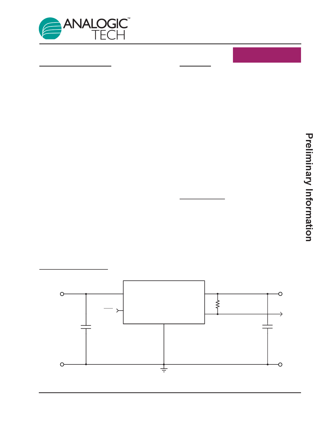
Typical Application
VIN
GND
IN
ON/OFF
EN
1µF
AAT3216
GND
OUT
POK
100k
VOUT
POK
2.2µF
GND
3216.2004.01.0.94
1
1 page 
AAT3216
150mA MicroPower™ LDO with PowerOK
Typical Characteristics
(Unless otherwise noted, VIN = 5V, TA = 25°C)
Dropout Voltage vs. Temperature
260
240
220
200
IL = 150mA
180
160
140
IL = 100mA
120
100
80
60
40 IL = 50mA
20
0
-40 -30 -20 -10 0 10 20 30 40 50 60 70 80 90 100 110 120
Temperature (°C)
Dropout Characteristics
3.20
3.00
IOUT = 0mA
2.80
2.60 IOUT = 10mA
IOUT = 50mA
2.40 IOUT = 100mA
2.20 IOUT = 150mA
2.00
2.70 2.80 2.90 3.00 3.10
VIN (V)
3.20
Dropout Voltage vs. Output Current
300
250
200
150
100
50
0
0
85°C
-40°C
25°C
25 50 75 100 125 150
Output Current (mA)
Quiescent Current vs. Temperature
100
90
80
70
60
50
40
30
20
10
0
-40 -30 -20 -10
0
10 20 30 40 50 60 70 80 90 100 110 120
Temperature (°C)
Ground Current vs. Input Voltage
90.00
80.00
70.00
60.00
50.00
40.00
30.00
IOUT=0mA
IOUT=150mA
IOUT=50mA
20.00
10.00
IOUT=10mA
0.00
2
2.5 3
3.5
VIN (V)
4
4.5
5
Output Voltage vs. Temperature
1.203
1.202
1.201
1.200
1.199
1.198
1.197
1.196
-40 -30 -20 -10 0 10 20 30 40 50 60 70 80 90 100
Temperature (°C)
3216.2004.01.0.94
5
5 Page 
AAT3216
150mA MicroPower™ LDO with PowerOK
Applications Information
The limiting characteristic for the maximum output
load current safe operating area is essentially
package power dissipation and the internal preset
thermal limit of the device. In order to obtain high
operating currents, careful device layout and circuit
operating conditions need to be taken into account.
The following discussions will assume the LDO reg-
ulator is mounted on a printed circuit board utilizing
the minimum recommended footprint as stated in
the layout considerations section of the document.
At any given ambient temperature (TA) the maxi-
mum package power dissipation can be deter-
mined by the following equation:
PD(MAX) = [TJ(MAX) - TA] / ΘJA
Constants for the AAT3216 are TJ(MAX), the maxi-
mum junction temperature for the device which is
125°C and ΘJA = 190°C/W, the package thermal
resistance. Typically, maximum conditions are cal-
culated at the maximum operating temperature
where TA = 85°C, under normal ambient conditions
TA = 25°C. Given TA = 85°, the maximum package
power dissipation is 211mW. At TA = 25°C°, the
maximum package power dissipation is 526mW.
The maximum continuous output current for the
AAT3216 is a function of the package power dissi-
pation and the input to output voltage drop across
the LDO regulator. Refer to the following simple
equation:
IOUT(MAX) < PD(MAX) / (VIN - VOUT)
For example, if VIN = 5V, VOUT = 3V and TA = 25°,
IOUT(MAX) < 264mA. If the output load current were to
exceed 264mA or if the ambient temperature were to
increase, the internal die temperature will increase.
If the condition remained constant, the LDO regula-
tor thermal protection circuit will activate.
To figure what the maximum input voltage would be
for a given load current refer to the following equa-
tion. This calculation accounts for the total power
dissipation of the LDO Regulator, including that
caused by ground current.
PD(MAX) = (VIN - VOUT)IOUT + (VIN x IGND)
This formula can be solved for VIN to determine the
maximum input voltage.
VIN(MAX) = (PD(MAX) + (VOUT x IOUT)) / (IOUT + IGND)
The following is an example for an AAT3216 set for
a 2.5 volt output:
From the discussion above, PD(MAX) was deter-
mined to equal 526mW at TA = 25°C.
VOUT = 2.5 volts
IOUT = 150mA
IGND = 150µA
VIN(MAX)=(526mW+(2.5Vx150mA))/(150mA +150µA)
VIN(MAX) = 6.00V
Thus, the AAT3216 can sustain a constant 2.5V
output at a 150mA load current as long as VIN is ≤
6.00V at an ambient temperature of 25°C. 6.0V is
the absolute maximum voltage where an AAT3216
would never be operated, thus at 25°C, the device
would not have any thermal concerns or opera-
tional VIN(MAX) limits.
This situation can be different at 85°C. The follow-
ing is an example for an AAT3216 set for a 2.5 volt
output at 85°C:
From the discussion above, PD(MAX) was deter-
mined to equal 211mW at TA = 85°C.
VOUT = 2.5 volts
IOUT = 150mA
IGND = 150uA
VIN(MAX)=(211mW+(2.5Vx150mA))/(150mA +150uA)
VIN(MAX) = 3.90V
Higher input to output voltage differentials can be
obtained with the AAT3216, while maintaining
device functions within the thermal safe operating
area. To accomplish this, the device thermal
resistance must be reduced by increasing the heat
sink area or by operating the LDO regulator in a
duty cycled mode.
For example, an application requires VIN = 4.2V
while VOUT = 2.5V at a 150mA load and TA = 85°C.
VIN is greater than 3.90V, which is the maximum
safe continuous input level for VOUT = 2.5V at
150mA for TA = 85°C. To maintain this high input
voltage and output current level, the LDO regulator
3216.2004.01.0.94
11
11 Page | ||
| Páginas | Total 16 Páginas | |
| PDF Descargar | [ Datasheet AAT3216IJS-2.7-T1.PDF ] | |
Hoja de datos destacado
| Número de pieza | Descripción | Fabricantes |
| AAT3216IJS-2.7-T1 | 150mA MicroPower LDO with PowerOK | ETC |
| Número de pieza | Descripción | Fabricantes |
| SLA6805M | High Voltage 3 phase Motor Driver IC. |
Sanken |
| SDC1742 | 12- and 14-Bit Hybrid Synchro / Resolver-to-Digital Converters. |
Analog Devices |
|
DataSheet.es es una pagina web que funciona como un repositorio de manuales o hoja de datos de muchos de los productos más populares, |
| DataSheet.es | 2020 | Privacy Policy | Contacto | Buscar |