|
|
|
PDF CS4954 Data sheet ( Hoja de datos )
| Número de pieza | CS4954 | |
| Descripción | NTSC/PAL Digital Video Encoder | |
| Fabricantes | Cirrus Logic | |
| Logotipo | ||
Hay una vista previa y un enlace de descarga de CS4954 (archivo pdf) en la parte inferior de esta página. Total 30 Páginas | ||
|
No Preview Available !
CS4954
CS4955
NTSC/PAL Digital Video Encoder
Features
Description
l Six DACs providing simultaneous composite,
S-video, and RGB or Component YUV
outputs
l Programmable DAC output currents for low
imped-ance (37.5 Ω) and high impedance
(150 Ω) loads.
l Multi-standard support for NTSC-M, NTSC-
JAPAN, PAL (B, D, G, H, I, M, N,
Combination N)
l ITU R.BT656 input mode supporting
EAV/SAV codes and CCIR601 Master/Slave
input modes
l Programmable HSYNC and VSYNC timing
l Multistandard Teletext (Europe, NABTS,
WST) support
l VBI encoding support
l Wide-Screen Signaling (WSS) support, EIA-J
CPX1204
l NTSC closed caption encoder with interrupt
l CS4955 supports Macrovision copy
protection Version 7
The CS4954/5 provides full conversion from digital video
formats YCbCr or YUV into NTSC and PAL Composite,
Y/C (S-video) and RGB, or YUV analog video. Input for-
mats can be 27 MHz 8-bit YUV, 8-bit YCbCr, or ITU
R.BT656 with support for EAV/SAV codes. Video output
can be formatted to be compatible with NTSC-M, NTSC-
J, PAL-B,D,G,H,I,M,N, and Combination N systems.
Closed Caption is supported in NTSC. Teletext is sup-
ported for NTSC and PAL.
Six 10-bit DACs provide two channels for an S-Video
output port, one or two composite video outputs, and
three RGB or YUV outputs. Two-times oversampling re-
duces the output filter requirements and guarantees no
DAC-related modulation components within the speci-
fied bandwidth of any of the supported video standards.
Parallel or high-speed I2C compatible control interfaces are
provided for flexibility in system design. The parallel interface
doubles as a general purpose I/O port when the CS4954/5 is
in I2C mode to help conserve valuable board area.
ORDERING INFORMATION
CS4954-CQ
CS4955-CQ
48-pin TQFP
48-pin TQFP
l Host interface configurable
for parallel or I2C
compatible operation
l On-chip voltage reference
generator
l +3.3 V or +5 V operation,
CMOS, low-power modes,
tri-state DACs
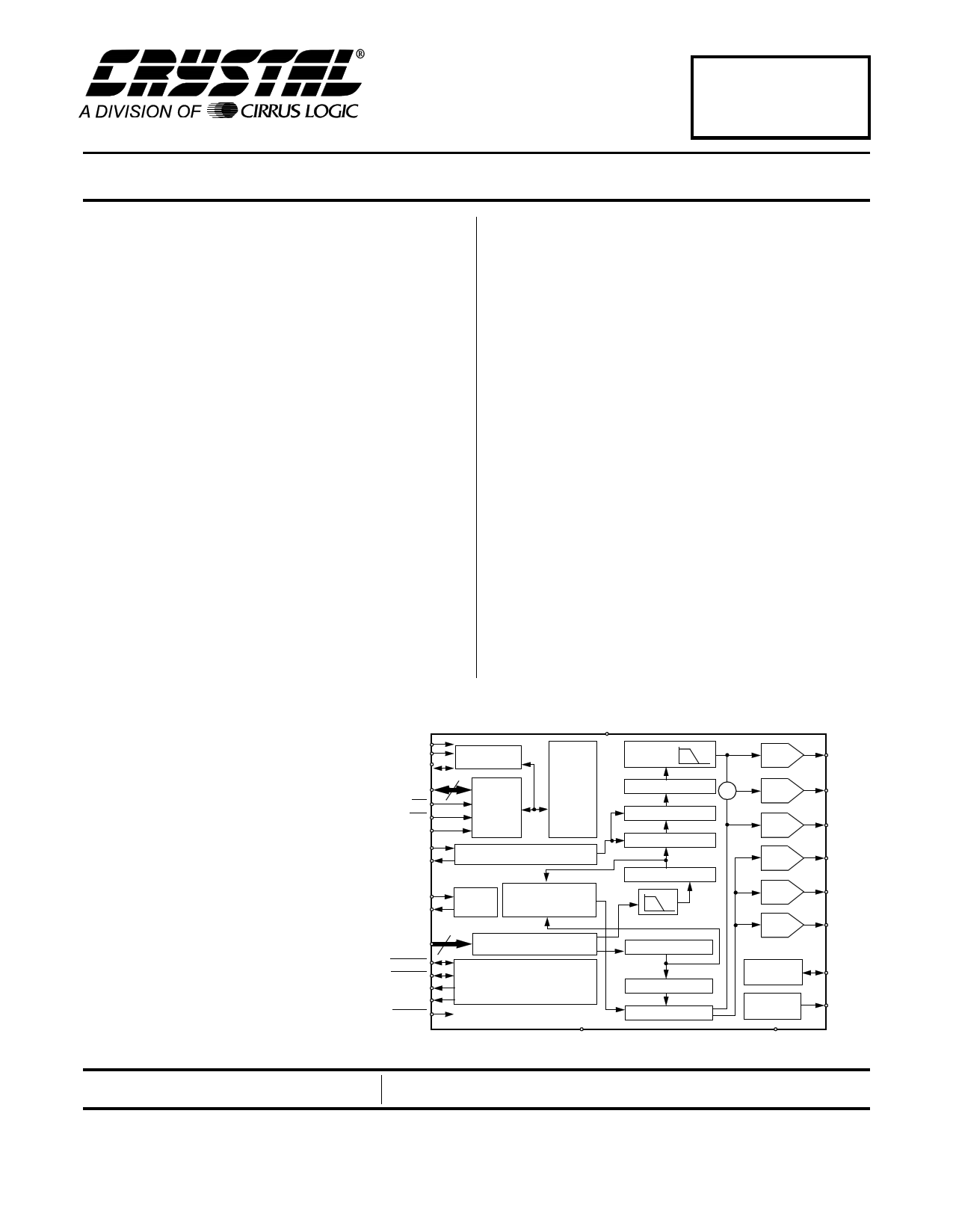
CLK
SCL
SDA
PDAT[7:0]
RD
WR
ADDR
XTAL_IN
XTAL_OUT
TTXDAT
TTXRQ
VD[7:0]
HSYNC
VSYNC
FIELD
INT
RESET
VAA
I2C Interface
Output LPF
Interpolate
10-Bit
DAC
8
Host
Parallel
Interface
Control
Registers
Color Sub-carrier Synthesizer
Teletext
Encoder
YCbCr to RBG
Color Space
Converter
8
Video Formatter
Chroma Amplifier Σ
Chroma Modulate
Burst Insert
Chroma Interpolate
U,V LPF
Y Luma Interpolate
10-Bit
DAC
10-Bit
DAC
10-Bit
DAC
10-Bit
DAC
10-Bit
DAC
Video Timing
Generator
RGB
Luma Amplifier
Y
Sync Insert
Y
RGB
Voltage
Reference
Current
Reference
C
CVBS
Y
R
G
B
VREF
ISET
DGND
TEST
Preliminary Product Information
Cirrus Logic, Inc.
P.O. Box 17847, Austin, Texas 78760
(512) 445 7222 FAX: (512) 445 7581
http://www.crystal.com
This document contains information for a new product.
Cirrus Logic reserves the right to modify this product without notice.
Copyright © Cirrus Logic, Inc. 1999
(All Rights Reserved)
APR ‘99
DS278PP4
1
1 page 
CS4954 CS4955
1. CHARACTERISTICS AND SPECIFICATIONS
ABSOLUTE MAXIMUM RATINGS
AC & DC PARAMETRIC SPECIFICATIONS (AGND,DGND = 0 V, all voltages with respect to 0 V)
Parameter
Symbol
Min
Max Units
Power Supply
VAA/VDD -0.3
6.0
V
Input Current Per Pin (Except Supply Pins)
-10 10 mA
Output Current Per Pin (Except Supply Pins)
-50 +50 mA
Analog Input Voltage
-0.3 VAA + 0.3
V
Digital Input Voltage
-0.3 VDD + 0.3
V
Ambient Temperature Power Applied
-55 + 125 °C
Storage Temperature
-65 + 150 °C
WARNING: Operating beyond these limits can result in permanent damage to the device. Normal operation is not
guaranteed at these extremes.
RECOMMENDED OPERATING CONDITIONS (AGND,DGND = 0 V, all voltages with respect to 0 V.)
Parameter
Power Supplies: Digital Analog
Operating Ambient Temperature
Symbol
VAA/VDD
TA
Min
3.15
4.75
0
Typ
3.3
5.0
+ 25
Max
3.45
5.25
+ 70
Units
V
°C
Note: Operation outside the ranges is not recommended.
DC CHARACTERISTICS (TA = 25° C; VAA, VDD = 5 V; GNDA, GNDD = 0 V.)
Parameter
Symbol Min Typ
Digital Inputs
High level Input Voltage
V [7:0], PDAT [7:0], Hsync/Vsync/Field/CLKIN
VIH 2.2 -
High Level Input Voltage I2C
VIH 0.7 VDD -
Low level Input Voltage All Inputs
- -0.3 -
Input Leakage Current
- -10 -
Digital Outputs
High Level Output Voltage lo = -4 mA
VOH
2.4
-
Low level Output Voltage lo = 4 mA
VOL - -
Low Level Output Voltage SDA pin only, lo = 6mA
VOL - -
Output Leakage Current High -Z Digital Outputs
- -10 -
Max Units
VDD+0.3 V
-V
0.8 V
+10 µA
VDD
0.4
0.4
+ 10
V
V
V
µA
DS278PP4
5
5 Page 
CS4954 CS4955
The CS4954/5 is designed to function as a video
timing master or video timing slave. In both Master
and Slave Modes, all timing is sampled and assert-
ed with the rising edge of the CLK pin.
In most cases, the CS4954/5 will serve as the video
timing master. HSYNC, VSYNC, and FIELD are
configured as outputs in Master Mode. HSYNC or
FIELD can also be defined as a composite blanking
output signal in Master Mode. In Master Mode, the
timing of HSYNC, VSYNC, FIELD and Compos-
ite Blank (CB) signals is programmable. Exact hor-
izontal and vertical display timing is addressed in
the Operational Description section.
In Slave Mode, HSYNC and VSYNC are typically
configured as input pins and are used to initialize
independent vertical and horizontal timing genera-
tors upon their respective falling edges. HSYNC
and VSYNC timing must conform to the ITU-
R BT.601 specifications.
The CS4954/5 also provides a ITU R.BT656 Slave
Mode in which the video input stream contains
EAV and SAV codes. In this case, proper HSYNC
and VSYNC timing are extracted automatically
without any inputs other than the V [7:0]. ITU
R.BT656 input data is sampled with the leading
edge of CLK.
In addition, it is also possible to output HSYNC
and VSYNC signals during CCIR-656 Slave
Mode.
4.2. Video Input Formatter
The Video Input Formatter translates YCbCr input
data into YUV information, when necessary, and
splits the luma and chroma information for filter-
ing, scaling, and modulation.
4.3. Color Subcarrier Synthesizer
The subcarrier synthesizer is a digital frequency
synthesizer that produces the appropriate subcarri-
er frequency for NTSC or PAL. The CS4954/5
generates the color burst frequency based on the
CLK input (27 MHz). Color burst accuracy and
stability are limited by the accuracy of the 27 MHz
input. If the frequency varies, then the color burst
frequency will also vary accordingly.
For environments in which the CLK input varies or
jitters unacceptably, a local crystal frequency refer-
ence can be used on the XTAL_IN and
XTAL_OUT pins. In this instance, the input CLK is
continuously compared with the external crystal ref-
erence input and the internal timing of the CS4954/5
is automatically adjusted so that the color burst fre-
quency remains within tolerance.
Controls are provided for phase adjustment of the
burst to permit color adjustment and phase com-
pensation. Chroma hue control is provided by the
CS4954/5 via a 10-bit Hue Control Register
(HUE_LSB and H_MSB). Burst amplitude control
is also made available to the host via the 8-bit burst
amplitude register (SC_AMP).
4.4. Chroma Path
The Video Input Formatter delivers 4:2:2 YUV
outputs into separate chroma and luma data paths.
The chroma path will be discussed here.
The chroma output of the Video Input Formatter is
directed to a chroma low-pass 19-tap FIR filter.
The filter bandwidth is selected (or the filter can be
bypassed) via the CONTROL_1 Register. The
passband of the filter is either 650 KHz or 1.3 MHz
and the passband ripple is less than or equal to
0.05 dB. The stopband for the 1.3 MHz selection
begins at 3 MHz with an attenuation of greater than
35 dB. The stopband for the 650 KHz selection be-
gins around 1.1 MHz with an attenuation of greater
than 20 dB.
The output of the chroma low-pass filter is connect-
ed to the chroma interpolation filter in which up-
sampling from 4:2:2 to 4:4:4 is accomplished.
Following the interpolation filter, the U and V
chroma signals pass through two independent vari-
able gain amplifiers in which the chroma amplitude
DS278PP4
11
11 Page | ||
| Páginas | Total 30 Páginas | |
| PDF Descargar | [ Datasheet CS4954.PDF ] | |
Hoja de datos destacado
| Número de pieza | Descripción | Fabricantes |
| CS4952 | NTSC/PAL Digital Video Encoder | Cirrus Logic |
| CS4953 | NTSC/PAL Digital Video Encoder | Cirrus Logic |
| CS495303 | Audio Decoder DSP Family | Cirrus Logic |
| CS495304 | Audio Decoder DSP Family | Cirrus Logic |
| Número de pieza | Descripción | Fabricantes |
| SLA6805M | High Voltage 3 phase Motor Driver IC. |
Sanken |
| SDC1742 | 12- and 14-Bit Hybrid Synchro / Resolver-to-Digital Converters. |
Analog Devices |
|
DataSheet.es es una pagina web que funciona como un repositorio de manuales o hoja de datos de muchos de los productos más populares, |
| DataSheet.es | 2020 | Privacy Policy | Contacto | Buscar |