|
|
|
PDF CS5106 Data sheet ( Hoja de datos )
| Número de pieza | CS5106 | |
| Descripción | Multi-Feature/ Synchronous plus Auxiliary PWM Controller | |
| Fabricantes | Cherry Semiconductor Corporation | |
| Logotipo | ||
Hay una vista previa y un enlace de descarga de CS5106 (archivo pdf) en la parte inferior de esta página. Total 12 Páginas | ||
|
No Preview Available !
CS5106
Multi-Feature, Synchronous plus Auxiliary
PWM Controller
Description
Features
The CS5106 is a fixed frequency,
current mode controller with one
single NFET driver and one dual
FET, synchronous driver. The syn-
chronous driver allows for
increased efficiency of the main iso-
lated power stage and the single
driver allows the designer to devel-
op auxiliary supplies for controller
power as well as secondary side
house keeping. In addition,
because the synchronous drivers
have programmable FET non-over-
lap, the CS5106 is an ideal con-
troller for soft-switched converter
topologies.
The CS5106 is specifically designed
for isolated topologies where speed,
flexibility, reduced size and
reduced component count are
requirements. The controller con-
tains the following features:
Undervoltage Shutdown,
Overvoltage Shutdown,
Programmable Frequency,
Programmable Synchronous Non-
Overlap Time, Master/Slave
Clocking with Frequency Range
Detection, Enable, Output
Undervoltage Protection with
Timer, 20mA 5V Output, 80ns
PWM propagation delay, and
Controlled Hiccup Mode.
The CS5106 has junction tempera-
ture and supply ranges of -40ûC to
125ûC and 9V to 16V respectively
and is available in the 24 lead SSOP
package.
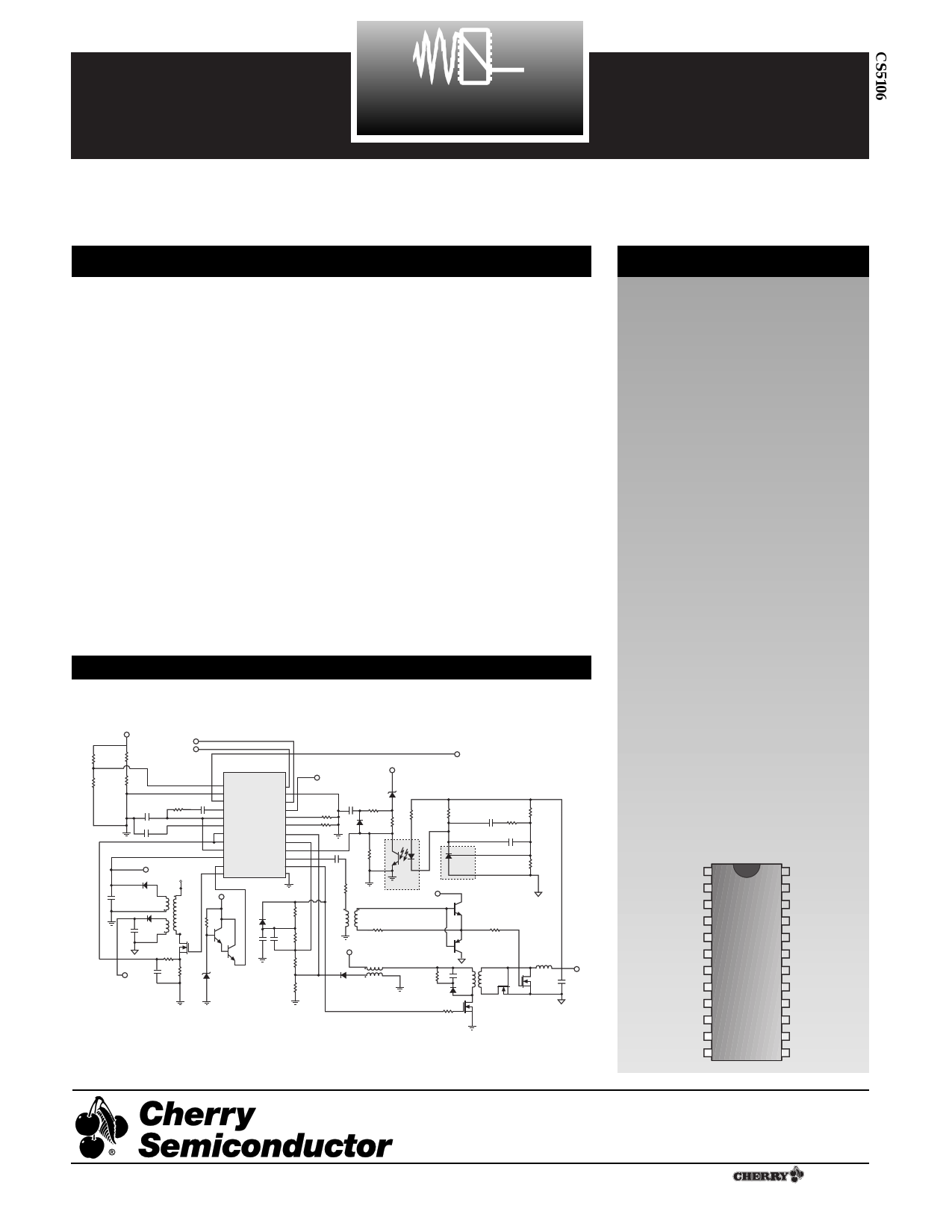
Applications Diagram
48V to 3.3V Forward Converter with Synchronous Rectifiers
R27
R3
VIN SYNCIN
ENABLE
R1
R2
C4
C1 R4
C2
VAUXP
D1
VIN
T1
CS5106
UVSD
ENABLE
OVSD PROGRAM
C3 V5REF SYNC IN
OAM
SYNC OUT
OAOUT
FADJ
OUVDELAY DLYSET
ILIM1
ILIM2
RAMP1
RAMP2
VFB1
VSS
VFB2
GATE2B
VCC
GATE1
GATE2
VDD
VIN
C5 D2
R5
R8
Q2
Q1
VAUXS C7 R6
D6
R9
D3
C9 C10 R10
R11
R12
SYNCOUT
VAUXP
V5REF
D5
C6 R7
R24
D8
R15
R20
R16 C14 R17
R25 C13
R14
C8
TL431
R13
T4
CNY17-4
VAUXS
Q7
R26
VIN
T3
D4
R21
Q6
R23
D7
T2
C11
Q3
R22
Q4
R18
R19
L1
Q5
VMAIN
C12
s Programmable Fixed
Frequency
s Programmable FET Non-
overlap
s Enable Lead
s 12V Fixed Auxiliary
Supply Control
s Under and Overvoltage
Shutdown
s Output Undervoltage
Protection with Timer
s Master/Slave Clock
Syncing Capability
s Sync Frequency Range
Detection
s 80ns PWM Propagation
Delay
s 20mA 5V Reference
Output
s Small 24 lead SSOP
Package
s Controlled Hiccup Mode
Package Options
24 Lead SSOP
UVSD 1
OVSD
V5REF
OAM
OAOUT
OUVDELAY
ILIM1
RAMP1
VFB1
VSS
VCC
GATE1
ENABLE
PROGRAM
SYNCIN
SYNCOUT
FADJ
DLYSET
ILIM2
RAMP2
VFB2
GATE2B
GATE2
VDD
Rev. 10/27/98
Cherry Semiconductor Corporation
2000 South County Trail, East Greenwich, RI 02818
Tel: (401)885-3600 Fax: (401)885-5786
Email: [email protected]
Web Site: www.cherry-semi.com
1 A ¨ Company
1 page 
Electrical Characteristics: TJ = -40¡C to 125¡C, VSS = 9 to 16V, V5REF ILOAD = 2mA, SYNCOUT Free Running, unless other-
wise specified. For All Specs: UVSD=6V, OVSD = 0V, ENABLE = 0V, ILIM(1,2) = 0,VFB(1,2) = 3V,RFADJ = RDLYSET = 27.4k½.
PARAMETER
s Current Limit Circuits
ILIM1 Current Limit Threshold
Voltage
ILIM1 Short Circuit Threshold
Voltage
ILIM1 Input Bias Current
ILIM2 Current Limit
Threshold V
ILIM2 Short Circuit
Threshold Voltage
ILIM2 Input Bias Current
s Voltage Feedback Control
RAMP1 Offset Voltage
RAMP1 Input Bias Current
RAMP2 Offset Voltage
RAMP2 Input Bias Current
VFB1 Input Impedance
VFB2 Input Impedance
s Gate1,2,2B Output Voltages
GATE1 Low State
GATE2 Low State
GATE2B Low State
GATE2B High State
GATE2 High State
GATE1 High State
TEST CONDITIONS
Adjust ILIM1 from 1.0V - 1.3V until
GATE1 goes low.
Adjust ILIM1 from 1.30V - 1.50V until
GATE1 skips 2-cycles with reference
to SYNCOUT.
Set ILIM1=0V. Measure current
out of ILIM1 lead.
Adjust ILIM2 from 1.0V - 1.3V until
GATE2 goes low.
Adjust ILIM2 from 1.30V - 1.50V until
GATE2 skips 2-cycles with reference
to SYNCOUT.
Set ILIM 2= 0V. Measure current out
of ILIM2 lead.
MIN
1.16
1.35
1.16
1.35
VFB1=0V. Adjust RAMP1 from 0V - 0.3V
until GATE1 goes low. Measure VRAMP1.
Set RAMP1 = 0V. Measure Current
out of RAMP1 lead.
VFB2 = 0V. Adjust RAMP2 from
0V-3V until GATE2 goes low.
Measure VRAMP2.
Set RAMP2 = 0V. Measure Current
out of RAMP2 lead.
Measure input impedance.
Measure Input impedance.
0.08
0.08
60.0
60.0
VSS = 12V. VCC = VSS - VDON
PROGRAM = 0V. Measure GATE1
voltage when sinking 1mA.
PROGRAM = 0V. Measure GATE2
voltage when sinking 1mA.
PROGRAM = 0V. Measure GATE2B
voltage when sinking 1mA.
Measure VCC - GATE2B voltage
when sourcing 1mA.
Measure VCC - GATE2 voltage
when sourcing 1mA.
Measure VCC - GATE1 voltage
when sourcing 1mA.
TYP
1.24
1.44
0.50
1.24
1.44
0.50
0.13
0.50
0.13
0.50
120.0
120.0
0.15
0.18
0.18
1.65
1.65
1.65
MAX
UNIT
1.30 V
1.51 V
5.00 µA
1.30 V
1.51 V
5.00 µA
0.20 V
5.00 µA
0.20 V
5.00
220.0
220.0
µA
k½
k½
0.80 V
0.80 V
0.80 V
2.00 V
2.00 V
2.00 V
s Propagation Delays
ILIM1 Delay to Output GATE1
Measure delay from ILIM1 going
high to GATE1 going low.
ILIM2 Delay to Output GATE2
Measure delay from ILIM2 going
high to GATE2 going low.
RAMP1 Delay to Output GATE1 Measure delay from RAMP1 going
high to GATE1 going low.
RAMP2 Delay to Output GATE2 Measure delay from RAMP2 going
high to GATE2 going low.
80.0 120.0 ns
80.0 100.0 ns
80.0 115.0 ns
80.0 100.0 ns
5
5 Page 
Theory of Application: continued
The equivalent down slope at the current sense resistor for
this application circuit is:
( )Slope @ R12 = Inductor_Slope ´
NST2
NPT2
´
NPT3
NST3
´ R12
V
µs
After choosing R9 and C9 to generate a ramp with a time
constant of about 5 times the oscillator period, R10 and R11
can be chosen for the voltage at RAMP2 to be 1.75 of the
voltage across R12.
Synchronous Rectification
Synchronous rectification was chosen to reduce losses in
the forward converter. Improvements in efficiency will be
most significant in low voltage, medium and high current
converters where improvement in conduction loss offsets
any added losses for gate drive.
In the application circuit Q4 is turned on and off by the for-
ward transformer. Q5 is turned on and off through pulse
transformer T4 and the gate driver formed by Q6 and Q7.
Because Q4 and Q5 are driven through different types of
components, differences in propagation delay must be con-
sidered. The DLYSET resistor should be chosen to avoid
shoot-through or excessive off time.
Gate Drive Capability
All GATE drive outputs have nominal peak currents of
0.5A. See Figures 6 and 7 for typical rise and fall times.
70
60
50
Rise Time
40
70
60
50
Rise Time
40
Fall Time
30
20
10
0
50
200
500
1000
1500
Load Capacitance (pF)
Figure 7: Typical GATE1 switching times.
2000
Design Considerations
The circuit board should utilize high frequency layout
techniques to avoid pulse width jitter and false triggering
of high impedance inputs. Ground plane(s) should be
employed. Signal grounds and power grounds should be
run separately. Portions of the circuit with high slew rates
or current pulses should be segregated from sensitive
areas. Shields and decoupling capacitors should be used as
required.
Special care should be taken to prevent coupling between
the SYNC leads and the surrounding leads. Depending on
the circuit board layout and component values, decoupling
capacitors or reduction in resistor values might be required
to reduce noise pick-up on the FADJ and DLYSET resistors.
Decoupling capacitors or active pull-up/down might be
required to prevent false triggering of the ENABLE and
PROGRAM leads.
30
20
Fall Time
10
0
50
100
200 500
1000
Load Capacitance (pF)
Figure 6: Typical GATE2, 2B switching times.
2000
11
11 Page | ||
| Páginas | Total 12 Páginas | |
| PDF Descargar | [ Datasheet CS5106.PDF ] | |
Hoja de datos destacado
| Número de pieza | Descripción | Fabricantes |
| CS5101 | Secondary Side Post Regulator for AC/DC and DC/DC Multiple Output Converters | Cherry Semiconductor Corporation |
| CS5101 | Secondary Side Post Regulator | ON Semiconductor |
| CS5101A | 16-Bit/ 100kHz/ 20kHz A/D Converters | Cirrus Logic |
| CS5101A-AL8 | 16-Bit/ 100kHz/ 20kHz A/D Converters | Cirrus Logic |
| Número de pieza | Descripción | Fabricantes |
| SLA6805M | High Voltage 3 phase Motor Driver IC. |
Sanken |
| SDC1742 | 12- and 14-Bit Hybrid Synchro / Resolver-to-Digital Converters. |
Analog Devices |
|
DataSheet.es es una pagina web que funciona como un repositorio de manuales o hoja de datos de muchos de los productos más populares, |
| DataSheet.es | 2020 | Privacy Policy | Contacto | Buscar |