|
|
|
PDF CS5127GDWR16 Data sheet ( Hoja de datos )
| Número de pieza | CS5127GDWR16 | |
| Descripción | Dual Output Nonsynchronous Buck Controller with Sync Function and Second Channel Enable | |
| Fabricantes | Cherry Semiconductor Corporation | |
| Logotipo | ||
Hay una vista previa y un enlace de descarga de CS5127GDWR16 (archivo pdf) en la parte inferior de esta página. Total 24 Páginas | ||
|
No Preview Available !
CS5127
Dual Output Nonsynchronous Buck Controller
with Sync Function and Second Channel Enable
Description
Features
The CS5127 is a fixed frequency
dual output nonsynchronous buck
controller. It contains circuitry for
regulating two separate outputs.
Each output channel contains a
high gain error amplifier, a com-
parator and latch, and a totem-pole
output driver capable of providing
DC current of 100mA and peak cur-
rent in excess of 0.5A. A common
oscillator controls switching for
both channels, and a sync lead is
provided to allow parallel supply
operation or shifting of the switch-
ing noise spectrum. An on-chip 5V
reference is capable of providing as
much as 10mA of current for exter-
nal circuitry. The CS5127 also
contains two undervoltage lockout
circuits. The first lockout releases
when VIN reaches 8.4V, while the
second lockout ensures that VREF is
higher than 3.6V. The outputs are
held in a low state until both lock-
outs have released. The controller is
configured to utilize the V2ª con-
trol method to achieve the fastest
possible transient response and
best overall regulation. This dual
controller is a cost-effective solu-
tion for providing VCORE and VIO
power solutions in computing
applications using a single con-
troller. The CS5127 will operate
over an input voltage range of 9.4V
to 20V and is available in a 16 lead
wide body surface mount package.
s Nonsynchronous Buck
Design
s V2ª Control Topology
s 100ns Transient Loop
Response
s Programmable Oscillator
Frequency
s 30ns Typical Gate Rise
and 10ns Fall Times
(No Load)
s Frequency
Synchronization Input
s ENABLE Input Controls
Channel 2 Gate Driver
s 5V/10mA Reference
Output
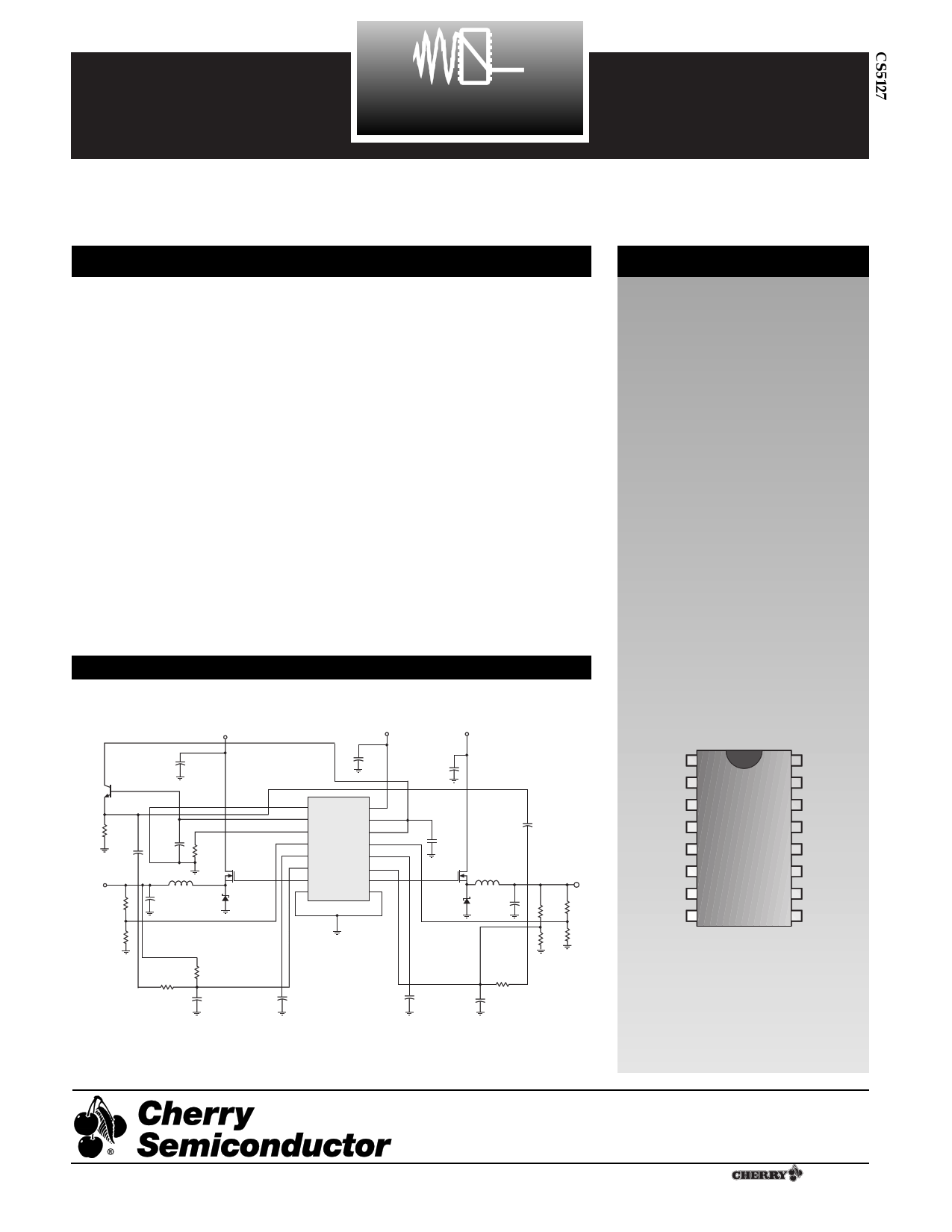
Applications Diagram
12V, 5V to 2.8V @ 7A and 3.3V @ 7A for 233MHz Pentium¨ Processor with MMXª Technology
5V
Q1
FMMT2222ACT
+ C1, C2
2 x 680mF
R1
20k
C6
0.1mF
2.8V
R4
1540
C7
330pF
R2
27k
L1
+ 5mH
C10, C11
2 x 680mF
Q2
IRL3103S
D1
1N5821
R5
1270
R6
R10 1k
20k C14
330pF
C3 +
1mF
12V +5V
C4, C5 +
2 x 680mF
SYNC
VIN
CS5127
CT VREF
RT ENABLE
VFB1
VFB2
COMP1
COMP2
VFFB1
VFFB2
GATE1
GATE2
LGnd
PGnd
+ C8
1mF
C9
0.1mF
Q3
IRL3103S
D2
1N5821
L2
5mH
C12, C13 +
2 x 680mF
C15
100mF
C16
100mF
C17
330pF
R11
20k
3.3V
R9
2k
R7
2400
R3
18k
R8
1500
Package Option
16 Lead SOIC Wide
SYNC 1
CT
RT
VFB1
COMP1
VFFB1
GATE1
LGND
VIN
VREF
ENABLE
VFB2
COMP2
VFFB2
GATE2
PGND
V2 is a trademark of Switch Power, Inc.
Pentium is a registered trademark and MMX is a trademark of Intel Corporation
Rev. 11/3/98
1
Cherry Semiconductor Corporation
2000 South County Trail, East Greenwich, RI 02818
Tel: (401)885-3600 Fax: (401)885-5786
Email: [email protected]
Web Site: www.cherry-semi.com
A ¨ Company
1 page 
Block Diagram
COMP1 VFFB1
VFB1
VREF
VIN
SYNC
RT
CT
VFB2
1.275V
-
Error
Amplifier
+
+
PWM
Comparator
-
VIN
Undervoltage
Lockout
Bandgap
Voltage
Reference
Reference
Undervoltage
Lockout
1.275V
+
Error
Amplifier
-
Oscillator
-
PWM
Comparator
+
Channel 2
Gate Driver
GATE1
LGND
PGND
Channel 2
Gate Driver
GATE2
COMP2 VFFB2
ENABLE
Theory of Operation
The CS5127 is a dual power supply controller that utilizes
the V2ª control method. Two nonsynchronous V2ª buck
regulators can be built using a single controller IC. This IC
is a perfect choice for efficiently and economically provid-
ing core power and I/O power for the latest
high-performance CPUs. Both switching regulators
employ a fixed frequency architecture driven from a
common oscillator circuit.
V2ª Control Method
The V2ª method of control uses a ramp signal generated
by the ESR of the output capacitors. This ramp is propor-
tional to the AC current in the inductor and is offset by the
DC output voltage. V2ª inherently compensates for varia-
tion in both line and load conditions since the ramp signal
is generated from the output voltage. This differs from tra-
ditional methods such as voltage mode control, where an
artificial ramp signal must be generated, and current mode
control, where a ramp is generated from inductor current.
+
PWM
Comparator
-
Ramp Signal
GATE
VFFB
COMP
-
Error
Amplifier
+
Error Signal
VFB
Reference
Voltage
Figure 1: V2ª control diagram.
The V2ª control method is illustrated in Figure 1. Both
the ramp signal and the error signal are generated by the
output voltage. Since the ramp voltage is defined as the
output voltage, the ramp signal is affected by any change
in the output, regardless of the origin of that change. The
ramp signal also contains the DC portion of the output
voltage, allowing the control circuit to drive the output
switch from 0% to about 90% duty cycle.
Changes in line voltage will change the current ramp in
the inductor, affecting the ramp signal and causing the
V2ª control loop to adjust the duty cycle. Since a change
in inductor current changes the ramp signal, the V2ª
method has the characteristics and advantages of current
mode control for line transient response.
Changes in load current will affect the output voltage and
thus will also change the ramp signal. A load step will
immediately change the state of the comparator output
that controls the output switch. In this case, load transient
response time is limited by the comparator response time
and the transition speed of the switch. Notice that the reac-
tion time of the V2ª loop to a load transient is not
dependent on the crossover frequency of the error signal
loop. Traditional voltage mode and current mode methods
are dependent on the compensation of the error signal
loop.
The V2ª error signal loop can have a low crossover fre-
quency, since transient response is handled by the ramp
signal loop. The ÒslowÓ error signal loop provides DC
accuracy. Low frequency roll-off of the error amplifier
bandwidth will significantly improve noise immunity.
This also improves remote sensing of the output voltage,
since switching noise picked up in long feedback traces
can be effectively filtered.
V2ª line and load regulation are dramatically improved
because there are two separate control loops. A voltage
5
5 Page 
Applications Information: continued
where TSOFT START is given in seconds if CCOMP is given in
farads, ICOMP(SOURCE) in amperes, and VFFB in volts. Note
that a design trade off will be made in choosing the value
of the COMP lead capacitor. Larger values of capacitance
will result in better regulation and improved noise immu-
nity, but the soft start interval will be longer and capacitor
price may increase.
VIN
CONTROL
LOGIC
L RL
C
VOUT
RA
RC R
PWM
VFFB
VR
VCONTROL
COMP
EA
C2
VFB
RB
R1
R2
C1
1.275V
Figure 6: Voltage mode control equivalent circuit with two pole, one
zero compensation network.
Figure 5: Measured performance of the CS5127 at start up.
CCOMP =100µF, ICOMP(SOURCE)=1.3mA, VFFB = 2.8V, TSOFTSTART = 0.22s.
Normal Operation
During normal operation, the gate driver switching duty
cycle will remain approximately constant as the V2ª con-
trol loop maintains the regulated output voltage under
steady state conditions. Changes in supply line or output
load conditions will result in changes in duty cycle to
maintain regulation.
Voltage Mode Control
VIN is the switch supply voltage, R represents the load, RL
is the combined resistance of the FET RDS (on) and the
inductor DC resistance, L is the inductor value, C is the
output capacitance, RC is the output capacitor ESR, RA
and RB are the feedback resistors and VR is the peak to
peak amplitude of the artificial ramp signal at the VFFB
pin. C1, C2, R1 and R2 are the components of the compen-
sation network. Based on the application circuit from page
1, values for the 2.8V output equivalent circuit are:
VIN =
R=
RL =
C=
RC =
RA =
RB =
L=
5V
0.4½
0.02½
1320µF
0.025½
1540½
1270½
5µH
Voltage Mode Operation
There are two methods by which a user can operate the
CS5127 in voltage mode. The first method is simple, but
the transient response is typically very poor. This method
uses the same components as V2ª operation, but by
increasing the amplitude of the artificial ramp signal, V2ª
control is defeated and the controller operates in voltage
mode. Calculate RR using the formula above and divide
the value obtained by 10. This should provide an ade-
quately large artificial ramp signal and cause operation
under voltage mode control. There may be some depen-
dence on board layout, and further optimization of the
value for RR may be done empirically if required.
Voltage mode control may be refined by removing the
COMP pin capacitor and adding a two pole, one zero com-
pensation network. Consider the system block diagram
shown in figure 6.
A resistor change is necessary to increase the artificial
ramp magnitude to VFFB1. Changing R10 from 20k to 2k
will give a peak to peak amplitude of about 2V. Thus, VR =
2V.
The transfer function from VCONTROL to VOUT is
VOUT
VCONTROL =
R ´ VIN ´ (sCRC + 1)
s2LC (R + RC) + s[L + RLC(R + RC) + RCRC] + R + RC
´
1
VR
Using the component values provided, this reduces to
11
11 Page | ||
| Páginas | Total 24 Páginas | |
| PDF Descargar | [ Datasheet CS5127GDWR16.PDF ] | |
Hoja de datos destacado
| Número de pieza | Descripción | Fabricantes |
| CS5127GDWR16 | Dual Output Nonsynchronous Buck Controller with Sync Function and Second Channel Enable | Cherry Semiconductor Corporation |
| Número de pieza | Descripción | Fabricantes |
| SLA6805M | High Voltage 3 phase Motor Driver IC. |
Sanken |
| SDC1742 | 12- and 14-Bit Hybrid Synchro / Resolver-to-Digital Converters. |
Analog Devices |
|
DataSheet.es es una pagina web que funciona como un repositorio de manuales o hoja de datos de muchos de los productos más populares, |
| DataSheet.es | 2020 | Privacy Policy | Contacto | Buscar |