|
|
|
PDF CS51312 Data sheet ( Hoja de datos )
| Número de pieza | CS51312 | |
| Descripción | Synchronous CPU Buck Controller for 12V Only Applications | |
| Fabricantes | Cherry Semiconductor Corporation | |
| Logotipo | ||
Hay una vista previa y un enlace de descarga de CS51312 (archivo pdf) en la parte inferior de esta página. Total 18 Páginas | ||
|
No Preview Available !
CS51312
Synchronous CPU Buck Controller
for 12V Only Applications
Description
Features
The CS51312 is a synchronous dual
NFET Buck Regulator Controller. It is
designed to power the core logic of
the latest high performance CPUs and
ASICs from a single 12V input. It uses
the V2TM control method to achieve
the fastest possible transient response
and best overall regulation. It incor-
porates many additional features
required to ensure the proper opera-
tion and protection of the CPU and
Power system. The CS51312 provides
the industry’s most highly integrated
solution, minimizing external compo-
nent count, total solution size, and
cost.
The CS51312 is specifically designed
to power Intel’s Pentium® II processor
and includes the following features:
5-bit DAC with 1.2% tolerance,
Power-Good output, overcurrent hic-
cup mode protection, overvoltage
protection, VCC monitor, Soft Start,
adaptive voltage positioning, adap-
tive FET non-overlap time, and
remote sense. The CS51312 will oper-
ate over a 9V to 20V (VCC2) range
using either single or dual input volt-
age and is available in 16 lead narrow
body surface mount package.
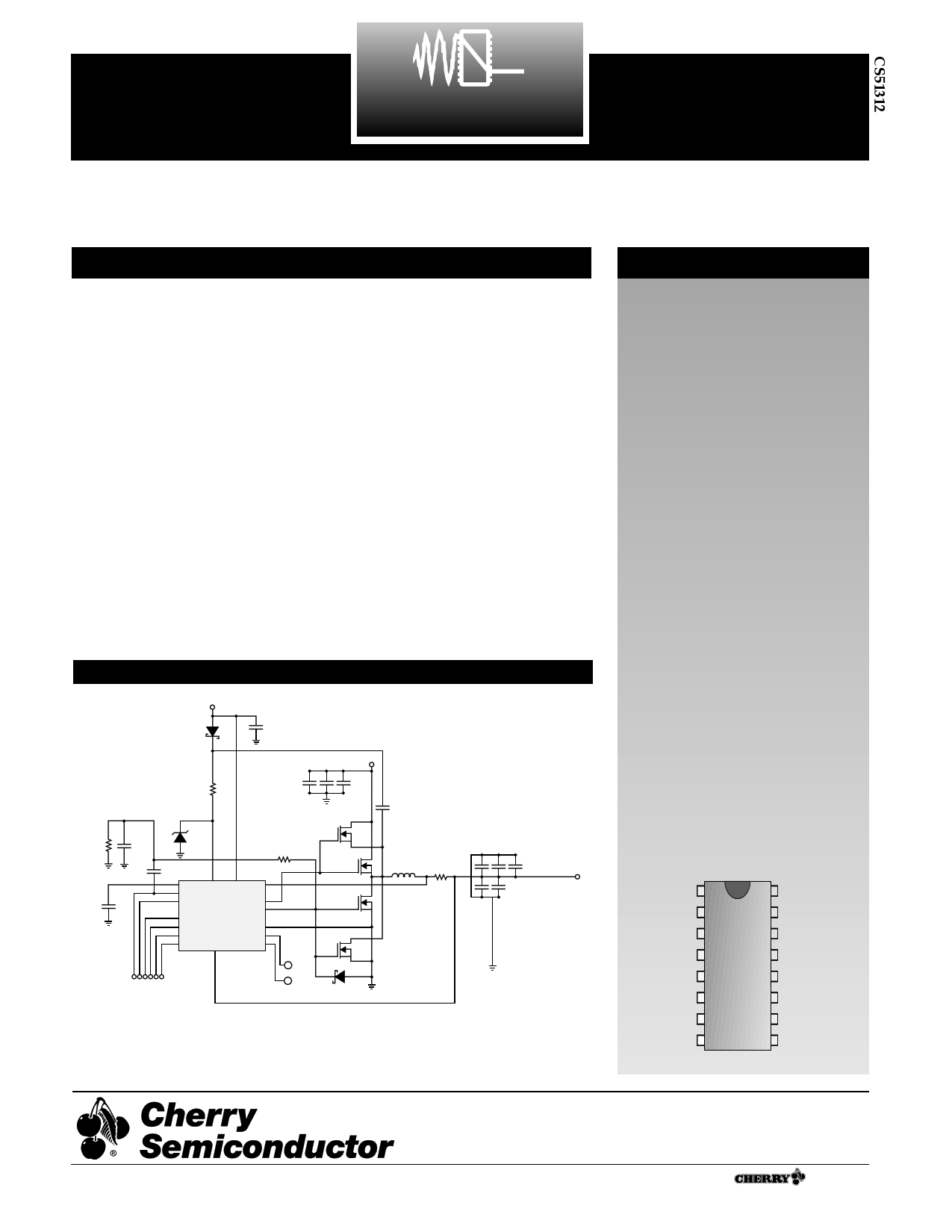
Application Diagram
12V
D1
SS16GICT-ND
C1
1.0µF
R2
200
C19
1000pF
12V
C2 C3 C4
R1
22Ω
D2
ZM4746ACT-ND
+++
220µF
16SV220
FY10AAJ-03A
C9
0.01µF
C10
1µF
R3
10k
98
15
16
1
2
3
4
5
COFF VCC2 VCC1 VFB
COMP
VID0 GATE(H)
GATE(L)
VID1 CS51312
VID2
Gnd
VID3
OVP
VID4 VOUT PWRGD
6
10
12
11
13
14
7 OVP
1
Q1
FY10AAJ-03A
Q2
FY10AAJ-03A
Q3
FY10AAJ-03A
Q4
DAC
1
PWRGD
D3
SS12GICT-ND
C6
0.010µF
L1 R4
1.2µH 0.004Ω
12V to 16A high performance converter.
C11 C12 C13
+ + + 470µF
+
+
470µF
1.25V to 3.5V
C14 C15 T510X477K006AS4394
V2 is a trademark of Switch Power, Inc.
Pentium is a registered trademark of Intel Corporation.
s Synchronous Switching
Regulator Controller for CPU
VCORE
s Dual N-Channel MOSFET
Synchronous Buck Design
s V2TM Control Topology
s 200ns Transient Loop Response
s 5 bit DAC with 1.2% Tolerance
s Hiccup Mode Overcurrent
Protection
s 40ns Gate Rise and Fall Times
(3.3nF load)
s 65ns Adaptive FET Non-overlap
Time
s Adaptive Voltage Positioning
s Power-Good Output Monitors
Regulator Output
s 5V/12V or 12V-only Operation
s VCC Monitor Provides Under
Voltage Lockout
s OVP Output Monitors Regulator
Output
s Multifunction COMP Pin
Provides ENABLE, Soft Start,
and Hiccup Timing in
Addition to Control Loop
Compensation
Package Options
16 Lead SO Narrow
VID0 1
VID1
VID2
VID3
VID4
VFB
VOUT
VCC1
COMP
COFF
PWRGD
OVP
GATE(L)
Gnd
GATE(H)
VCC2
Rev. 3/11/99
Cherry Semiconductor Corporation
2000 South County Trail, East Greenwich, RI 02818
Tel: (401)885-3600 Fax: (401)885-5786
Email: [email protected]
Web Site: www.cherry-semi.com
1 A ® Company
1 page 
2.0V
DAC
Electrical Characteristics: 0˚C <
Code(VID4 = VID3 =VID2 = VID1 = 0,
VTAID<0
=701˚)C, ;C0G˚CAT<E(HT)J
<
=
C12G5A˚TCE;(L9)V=<3.V3nCFC,1
< 14V;
COFF =
399V0p≤FV; CUCn2l≤es2s0oVt;herwise
stated.
PARAMETER
TEST CONDITIONS
s General Electrical Specifications
VCC1 Monitor Start Threshold
VCC1 Monitor Stop Threshold
Hysteresis
Start - Stop
VCC1 Supply Current
No Load on GATE(H), GATE(L)
VCC2 Supply Current
No Load on GATE(H), GATE(L)
MIN
7.9
7.6
0.15
TYP
8.4
8.1
0.30
9.5
2.5
MAX
8.9
8.6
0.60
16
4.5
UNIT
V
V
V
mA
mA
Note 1: The IC power dissipation in a typical application with VCC = 12V, switching frequency fSW = 250kHz, 50nc
MOSFETs and RθJA = 115°C/W yields an operating junction temperature rise of approximately 52°C, and a junction tem-
perature of 77°C with an ambient temperature of 25°C.
Note 2: Guaranteed by design, not 100% tested in production.
Block Diagram
VOUT
VID0
VID1
VID2
VID3
VID4
VFB
1.1V
-
COMP
EA
PWM COMP
+
-
CURRENT LIMIT
86mV
-
+
-
DISCHARGE
COMP
R
+- 0.25V
Q
FAULT
LATCH
S
COFF
OFF
TIME
DAC
UVLO
VCC1
VCC2
GATE(H)
NONOVERLAP
+ LOGIC
-
+
-
VCC1
OVP
PWRGD
5
GATE(L)
Gnd
5 Page 
Application Information: continued
where
∆I/∆T = load current slew rate (as high as 20A/µs);
∆VESL = change in output voltage due to ESL.
The actual maximum allowable ESL can be determined by
using the equation:
ESLMAX =
ESLCAP
Number of output capacitors
,
where ESLCAP = maximum ESL per capacitor (it is estimat-
ed that a 10 × 12mm Aluminum Electrolytic capacitor has
approximately 4nH of package inductance).
The actual output voltage deviation due to the actual maxi-
mum ESL can then be verified:
∆VESL =
ESLMAX × ∆I
∆t
.
The designer now must determine the change in output
voltage due to output capacitor discharge during the tran-
sient:
∆VCAP =
∆I × ∆tTR
COUT
,
where
∆tTR = the output voltage transient response time
(assigned by the designer);
∆VCAP = output voltage deviation due to output capaci-
tor discharge;
∆I = Load step.
The total change in output voltage as a result of a load cur-
rent transient can be verified by the following formula:
∆VOUT = ∆VESR + ∆VESL + ∆VCAP
Step 3: Selection of the Duty Cycle,
Switching Frequency, Switch On-Time (TON)
and Switch Off-Time (TOFF)
The duty cycle of a buck converter (including parasitic
losses) is given by the formula:
Duty Cycle = D =
VOUT + (VHFET + VL + VDROOP)
VIN + VLFET − VHFET − VL
,
where
VOUT = buck regulator output voltage;
VHFET = high side FET voltage drop due to RDS(ON);
VL = output inductor voltage drop due to inductor wire
DC resistance;
VDROOP = droop (current sense) resistor voltage drop;
VIN = buck regulator input voltage;
VLFET = low side FET voltage drop due to RDS(ON).
Step3a: Calculation of Switch On-Time
The switch On-Time (time during which the switching
MOSFET in a synchronous buck topology is conducting) is
determined by:
TON =
Duty Cycle
FSW
,
where FSW = regulator switching frequency selected by the
designer.
Higher operating frequencies allow the use of smaller
inductor and capacitor values. Nevertheless, it is common
to select lower frequency operation because a higher fre-
quency results in lower efficiency due to MOSFET gate
charge losses. Additionally, the use of smaller inductors at
higher frequencies results in higher ripple current, higher
output voltage ripple, and lower efficiency at light load
currents.
Step 3b: Calculation of Switch Off-Time
The switch Off-Time (time during which the switching
MOSFET is not conducting) can be determined by:
TOFF =
1
FSW
− TON,
The COFF capacitor value has to be selected in order to set
the Off-Time, TOFF, above:
COFF =
Period × (1 − D) ,
3980
where
3980 is a characteristic factor of the CS51312;
D = Duty Cycle.
Step 4: Selection of the Output Inductor
The inductor should be selected based on its inductance,
current capability, and DC resistance. Increasing the induc-
tor value will decrease output voltage ripple, but degrade
transient response. There are many factors to consider in
selecting the inductor including cost, efficiency, EMI and
ease of manufacture. The inductor must be able to handle
the peak current at the switching frequency without satu-
rating, and the copper resistance in the winding should be
kept as low as possible to minimize resistive power loss.
There are a variety of materials and types of magnetic
cores that could be used for this application. Among them
are ferrites, molypermalloy cores (MPP), amorphous and
powdered iron cores. Powdered iron cores are very com-
monly used. Powdered iron cores are very suitable due to
their high saturation flux density and have low loss at high
frequencies, a distributed gap and exhibit very low EMI.
The inductor value can be determined by:
L = (VIN − VOUT) × tTR ,
∆Ι
where
VIN = input voltage;
VOUT = output voltage;
tTR = output voltage transient response time (assigned
by the designer);
∆I = load transient.
The inductor ripple current can then be determined:
∆IL =
VOUT ×
L
TOFF
,
11
11 Page | ||
| Páginas | Total 18 Páginas | |
| PDF Descargar | [ Datasheet CS51312.PDF ] | |
Hoja de datos destacado
| Número de pieza | Descripción | Fabricantes |
| CS51311 | Synchronous CPU Buck Controller for 12V and 5V Applications | Cherry Semiconductor Corporation |
| CS51311 | Synchronous CPU Buck Controller | ON Semiconductor |
| CS51311GD14 | Synchronous CPU Buck Controller for 12V and 5V Applications | Cherry Semiconductor Corporation |
| CS51311GDR14 | Synchronous CPU Buck Controller for 12V and 5V Applications | Cherry Semiconductor Corporation |
| Número de pieza | Descripción | Fabricantes |
| SLA6805M | High Voltage 3 phase Motor Driver IC. |
Sanken |
| SDC1742 | 12- and 14-Bit Hybrid Synchro / Resolver-to-Digital Converters. |
Analog Devices |
|
DataSheet.es es una pagina web que funciona como un repositorio de manuales o hoja de datos de muchos de los productos más populares, |
| DataSheet.es | 2020 | Privacy Policy | Contacto | Buscar |