|
|
PDF CS5150GDR16 Data sheet ( Hoja de datos )
| Número de pieza | CS5150GDR16 | |
| Descripción | CPU 4-Bit Synchronous Buck Controller | |
| Fabricantes | Cherry Semiconductor Corporation | |
| Logotipo | ||
Hay una vista previa y un enlace de descarga de CS5150GDR16 (archivo pdf) en la parte inferior de esta página. Total 14 Páginas | ||
|
No Preview Available !
CS5150
CPU 4-Bit Synchronous Buck Controller
Description
Features
The CS5150 is a 4-bit synchronous
dual N-Channel buck controller. It
is designed to provide unprece-
dented transient response for
today’s demanding high-density,
high-speed logic. The regulator
operates using a proprietary control
method, which allows a 100ns
response time to load transients.
The CS5150 is designed to operate
over a 4.25-16V range (VCC) using
12V to power the IC and 5V as the
main supply for conversion.
The CS5150 is specifically designed
to power Pentium® Pro processors
and other high performance core
logic. It includes the following fea-
tures: on board, 4-bit DAC, short
circuit protection, 1.0% output tol-
erance, VCC monitor, and pro-
grammable soft start capability. The
CS5150 is upward compatible with
the 5-bit CS5155, allowing the
mother board designer the capabili-
ty of using either the CS5150 or the
CS5155 with no change in layout.
The CS5150 is available in 16 pin
surface mount and DIP packages.
Application Diagram
Switching Power Supply for core logic - Pentium® Pro processor
12V 5V
0.1µF
VID0
VID1
VID2
VID3
330pF
VCC1
VCC2
VGATE(H)
VID0
VID1
VID2
VID3
CS5150
VGATE(L)
COFF
PGnd
0.1µF
SS
COMP
0.33µF
LGnd
VFB
VFFB
3.3k
100pF
1200µF/16V x 3
AlEl
IRL3103
2µH
2.1V to 3.5V @ 13A
IRL3103
1200µF/16V x 5
AlEl
s Dual N-Channel Design
s Excess of 1MHz Operation
s 100ns Transient Response
s 4-Bit DAC
s Upward Compatible with
5-Bit CS5155/5156 and
Adjustable CS5120/5121
s 30ns Gate Rise/Fall Times
s 1% DAC Accuracy
s 5V & 12V Operation
s Remote Sense
s Programmable Soft Start
s Lossless Short Circuit
Protection
s VCC Monitor
s 25ns FET Nonoverlap Time
s Adaptive Voltage
Positioning
s V2™ Control Topology
s Current Sharing
s Overvoltage Protection
Package Options
16 Lead SO Narrow & PDIP
VID0 1
VID1
VID2
VID3
SS
NC
COFF
VFFB
VFB
COMP
LGnd
VCC1
VGATE(L)
PGnd
VGATE(H)
VCC2
V2 is a trademark of Switch Power, Inc.
Pentium is a registered trademark of Intel Corporation.
Rev. 1/4/99
Cherry Semiconductor Corporation
2000 South County Trail, East Greenwich, RI 02818
Tel: (401)885-3600 Fax: (401)885-5786
Email: [email protected]
Web Site: www.cherry-semi.com
1 A ® Company
1 page 
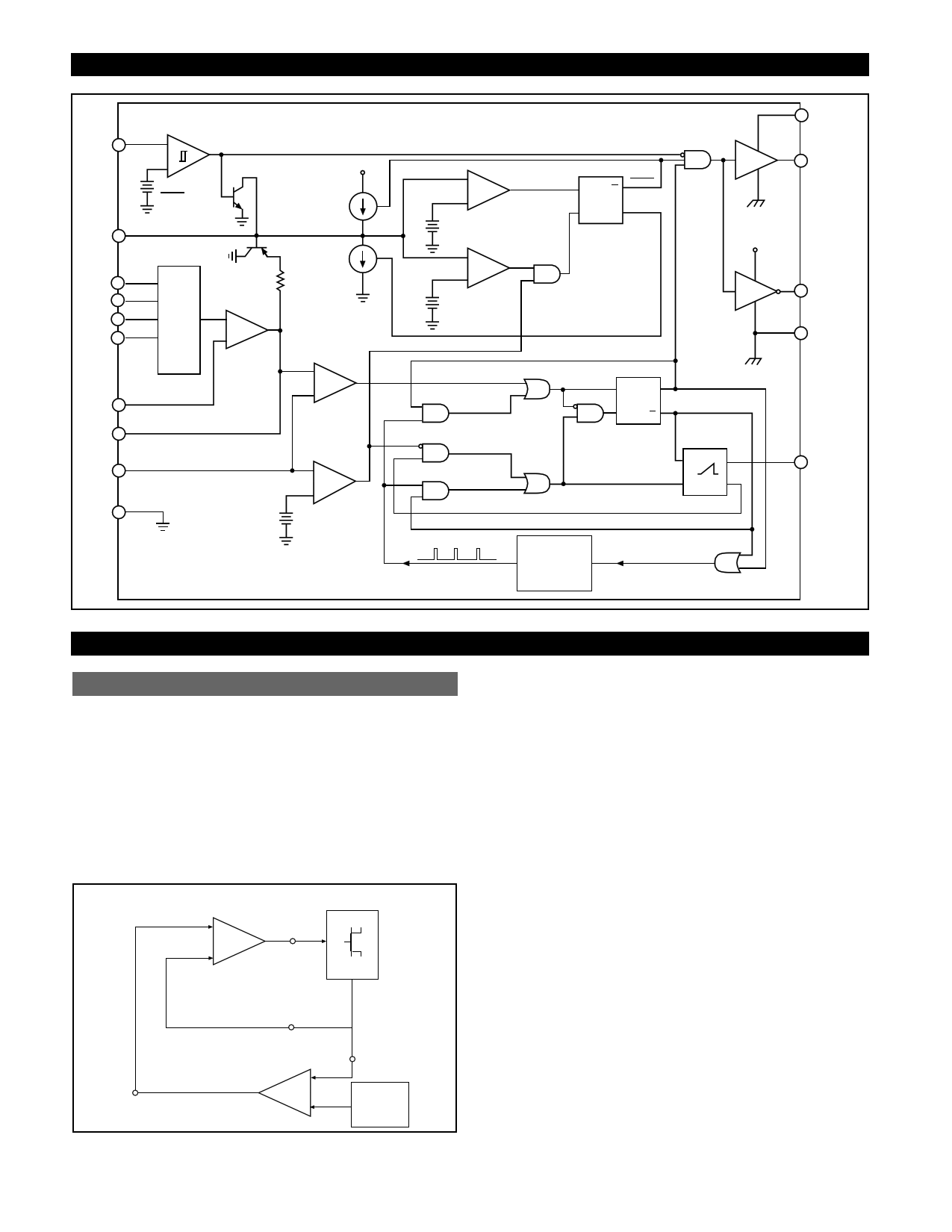
Block Diagram
VCC1
SS
VID0
VID1
VID2
VID3
VFB
COMP
VFFB
LGnd
VCC1 Monitor
Comparator
-
+
3.90V
3.85V
5V
60µA
2µA
4 BIT
DAC
Error
+ Amplifier
-
Slow Feedback
PWM
Comparator
-
+
Fast Feedback
-
+
VFFB Low
1V Comparator
PWM
COMP
2.5V
SS Low
- Comparator
+
0.7V
SS High
+ Comparator
-
Maximum
On-Time
Timeout
Normal
Off-Time
Timeout
Extended
Off-Time
Timeout
FAULT
RQ
S Q FAULT
FAULT
Latch
VCC2
VGATE(H)
PGnd
VCC1
VGATE(L)
PGnd
RQ
SQ
PWM
Latch
Off-Time
Timeout
GATE(H) = ON
GATE(H) = OFF
COFF
One Shot
R
SQ
COFF
Time Out
Timer
(30µs)
Edge Triggered
Applications Information
Theory of Operation
V2™ Control Method
The V2™ method of control uses a ramp signal that is gen-
erated by the ESR of the output capacitors. This ramp is
proportional to the AC current through the main inductor
and is offset by the value of the DC output voltage. This
control scheme inherently compensates for variation in
either line or load conditions, since the ramp signal is gen-
erated from the output voltage itself. This control scheme
differs from traditional techniques such as voltage mode,
which generates an artificial ramp, and current mode,
which generates a ramp from inductor current.
PWM
Comparator
C
–
VGATE(H)
VGATE(L)
Ramp
Signal
VFFB
COMP
Error
Amplifier
–
Error
Signal
E
+
Figure 1: V2™ Control Diagram
Output
Voltage
Feedback
VFB
Reference
Voltage
The V2™ control method is illustrated in Figure 1. The out-
put voltage is used to generate both the error signal and the
ramp signal. Since the ramp signal is simply the output
voltage, it is affected by any change in the output regard-
less of the origin of that change. The ramp signal also con-
tains the DC portion of the output voltage, which allows
the control circuit to drive the main switch to 0% or 100%
duty cycle as required.
A change in line voltage changes the current ramp in the
inductor, affecting the ramp signal, which causes the V2™
control scheme to compensate the duty cycle. Since the
change in inductor current modifies the ramp signal, as in
current mode control, the V2™ control scheme has the
same advantages in line transient response.
A change in load current will have an affect on the output
voltage, altering the ramp signal. A load step immediately
changes the state of the comparator output, which controls
the main switch. Load transient response is determined
only by the comparator response time and the transition
speed of the main switch. The reaction time to an output
load step has no relation to the crossover frequency of the
error signal loop, as in traditional control methods.
The error signal loop can have a low crossover frequency,
since transient response is handled by the ramp signal loop.
The main purpose of this ‘slow’ feedback loop is to provide
DC accuracy. Noise immunity is significantly improved,
since the error amplifier bandwidth can be rolled off at a low
frequency. Enhanced noise immunity improves remote sens-
5
5 Page 
Applications Information: continued
COFF timing capacitor:
COFF
=
Period × (1 - duty cycle)
4848.5
,
where:
Period =
1
switching frequency
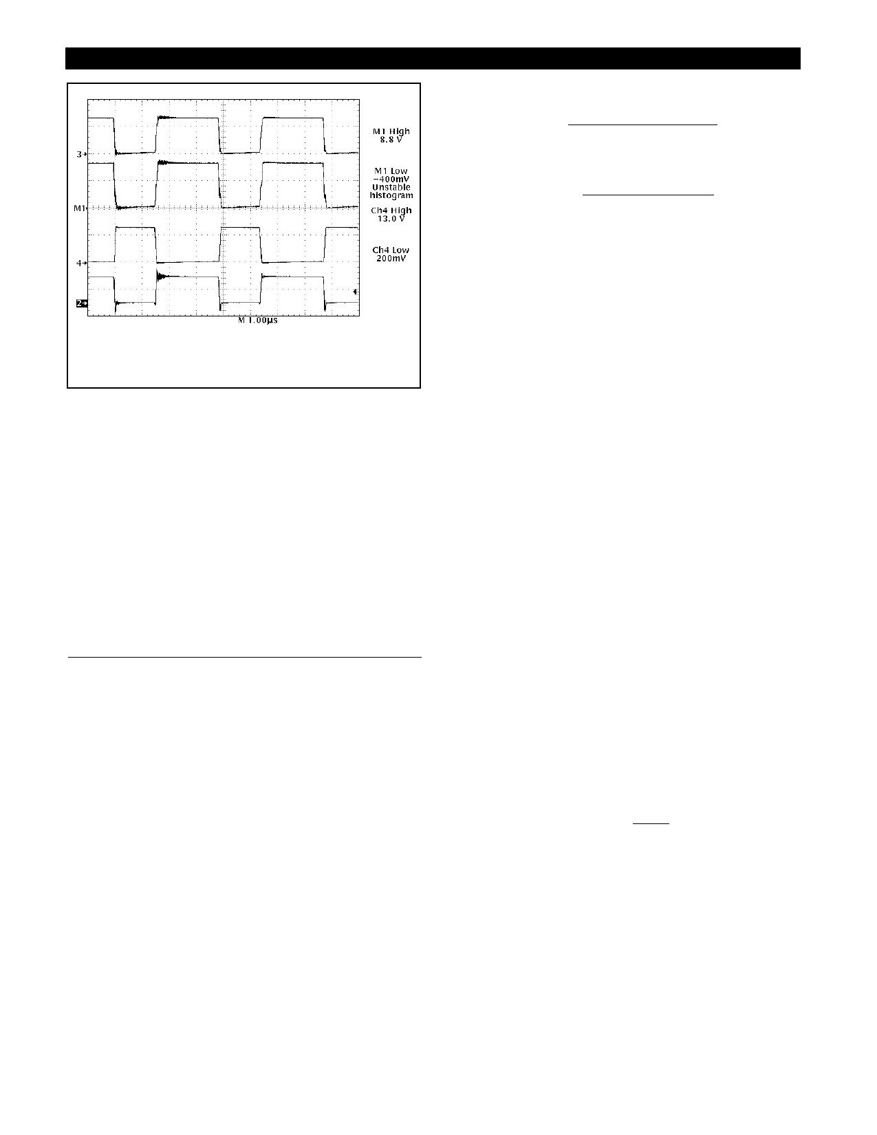
Trace 3 = VGATE(H) (10V/div.)
Math 1= VGATE(H) - 5VIN
Trace 4 = VGATE(L) (10V/div.)
Trace 2 = Inductor Switching Node (5V/div.)
Figure 17: CS5150 gate drive waveforms depicting rail to rail swing.
The most important aspect of MOSFET performance is
RDSON, which effects regulator efficiency and MOSFET
thermal management requirements.
The power dissipated by the MOSFETs may be estimated
as follows;
Switching MOSFET:
Power = ILOAD2 × RDSON × duty cycle
Schottky Diode for Synchronous MOSFET
A Schottky diode may be placed in parallel with the syn-
chronous MOSFET to conduct the inductor current upon
turn off of the switching MOSFET to improve efficiency.
The CS5150 reference circuit does not use this device due to
its excellent design. Instead, the body diode of the syn-
chronous MOSFET is utilized to reduce cost and conducts
the inductor current. For a design operating at 200kHz or so,
the low non-overlap time combined with Schottky forward
recovery time may make the benefits of this device not
worth the additional expense (see Figure 6, channel 2). The
power dissipation in the synchronous MOSFET due to body
diode conduction can be estimated by the following equation:
Power = Vbd × ILOAD × conduction time × switching frequency
Where Vbd = the forward drop of the MOSFET body diode.
For the CS5150 demonstration board as shown in Figure 6;
Power = 1.6V × 13A × 100ns × 233kHz = 0.48W
Synchronous MOSFET:
Power = ILOAD2 × RDSON × (1 - duty cycle)
Duty Cycle =
VOUT + (ILOAD × RDSON OF SYNCH FET)
VIN + (ILOAD × RDSON OF SYNCH FET) - (ILOAD × RDSON OF SWITCH FET)
Off Time Capacitor (COFF)
The COFF timing capacitor sets the regulator off time:
TOFF = COFF × 4848.5
When the VFFB pin is less than 1V, the current charging the
COFF capacitor is reduced. The extended off time can be cal-
culated as follows:
TOFF = COFF × 24,242.5.
Off time will be determined by either the TOFF time, or the
time out timer, whichever is longer.
The preceding equations for duty cycle can also be used to
calculate the regulator switching frequency and select the
This is only 1.3% of the 36.4W being delivered to the load.
“Droop” Resistor for Adaptive Voltage Positioning
Adaptive voltage positioning is used to reduce output volt-
age excursions during abrupt changes in load current.
Regulator output voltage is offset +40mV when the regula-
tor is unloaded, and -40mV at full load. This results in
increased margin before encountering minimum and maxi-
mum transient voltage limits, allowing use of less capaci-
tance on the regulator output (see Figure 7).
To implement adaptive voltage positioning, a “droop”
resistor must be connected between the output inductor
and output capacitors and load. This is normally imple-
mented by a PC board trace of the following value:
RDROOP
=
80mV
IMAX
Adaptive voltage positioning can be disabled for improved
DC regulation by connecting the VFB pin directly to the load
using a separate, non-load current carrying circuit trace.
11
11 Page | ||
| Páginas | Total 14 Páginas | |
| PDF Descargar | [ Datasheet CS5150GDR16.PDF ] | |
Hoja de datos destacado
| Número de pieza | Descripción | Fabricantes |
| CS5150GDR16 | CPU 4-Bit Synchronous Buck Controller | Cherry Semiconductor Corporation |
| Número de pieza | Descripción | Fabricantes |
| SLA6805M | High Voltage 3 phase Motor Driver IC. |
Sanken |
| SDC1742 | 12- and 14-Bit Hybrid Synchro / Resolver-to-Digital Converters. |
Analog Devices |
|
DataSheet.es es una pagina web que funciona como un repositorio de manuales o hoja de datos de muchos de los productos más populares, |
| DataSheet.es | 2020 | Privacy Policy | Contacto | Buscar |
