|
|
|
PDF CS5165 Data sheet ( Hoja de datos )
| Número de pieza | CS5165 | |
| Descripción | Fast/ Precise 5-Bit Synchronous Buck Controller for the Next Generation Low Voltage Pentium II Processors | |
| Fabricantes | Cherry Semiconductor Corporation | |
| Logotipo | ||
Hay una vista previa y un enlace de descarga de CS5165 (archivo pdf) en la parte inferior de esta página. Total 19 Páginas | ||
|
No Preview Available !
CS5165
Fast, Precise 5-Bit Synchronous Buck Controller
for the Next Generation Low Voltage Pentium® II Processors
Description
Features
The CS5165 synchronous 5-bit NFET
buck controller is optimized to manage
the power of the next generation
Pentium®II processors. It’s V2™ control
architecture delivers the fastest transient
response (100ns), and best overall voltage
regulation in the industry today. It’s fea-
ture rich design gives end users the maxi-
mum flexibility to implement the best
price/performance solutions for their end
products.
The CS5165 has been carefully crafted to
maximize performance and protect the
processor during operation. It has a 5-bit
DAC on board that holds a ±1% tolerance
over temperature. Its on board pro-
grammable soft start insures a control
start up, and the FET nonoverlap circuit-
ry ensures that both FETs do not conduct
simultaneously.
The on board oscillator can be pro-
grammed up to 1MHz to give the design-
er maximum flexibility in choosing exter-
nal components and setting systems costs.
The CS5165 protects the processor during
potentially catastrophic events like over-
voltage (OVP) and short circuit. The OVP
feature is part of the V2™ architecture and
does not require any additional compo-
nents. During short circuit, the controller
pulses the MOSFETs in a “hiccup” mode
(3% duty cycle) until the fault is removed.
With this method, the MOSFETs do not
overheat or self destruct.
The CS5165 is designed for use in both
single processor desktop and multipro-
cessor workstation and server applica-
tions. The CS5165’s current sharing capa-
bility allows the designer to build multi-
ple parallel and redundant power solu-
tions for multiprocessor systems.
The CS5165 contains other control and
protection features such as Power Good,
ENABLE, and adaptive voltage position-
ing. It is available in a 16 lead SOIC wide
body package.
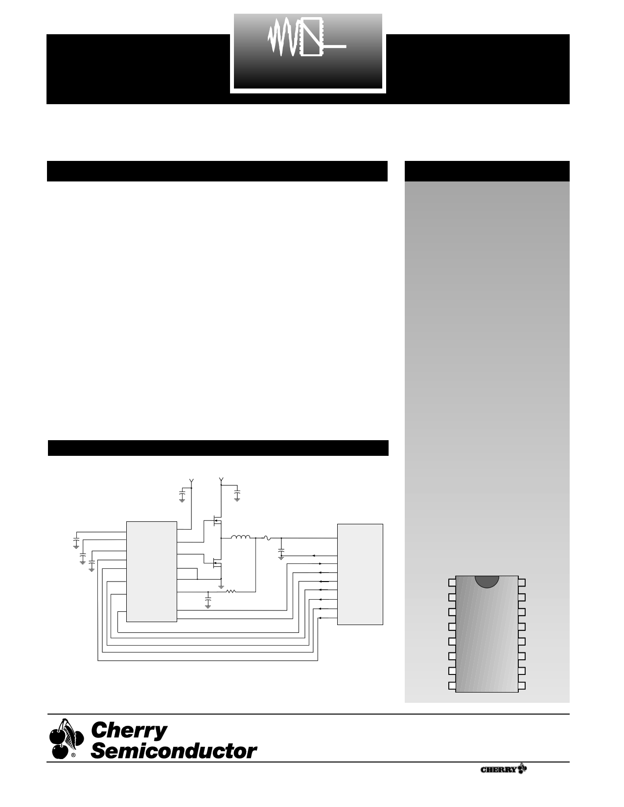
Application Diagram
5V to 2.8V @ 14.2A for 300MHz Pentium®II
12V
5V
1µF 1200µF/10V x 3
s V2™ Control Topology
s Dual N Channel Design
s 100ns Controller Transient
Response
s Excess of 1Mhz Operation
s 5 Bit DAC with 1% Tolerance
s Power Good Output With
Internal Delay
s Enable Input Provides
Micropower Shutdown Mode
s Complete Pentium® II System
Requires 18 Components
s 5V and 12V Operation
s Adaptive Voltage Positioning
s Remote Sense Capability
s Current Sharing Capability
s VCC Monitor
s Hiccup Mode Short Circuit
Protection
s Overvoltage Protection (OVP)
s Programmable Soft Start
s 150ns PWM Blanking
s 65ns FET Non-Overlap
s 40ns Gate Rise and Fall Times
(3.3nF load)
0.1µF
0.1 µF
330pF
SS
COMP
COFF
VID4
VID3
VID2
VID1
CS5165
VID0
VCC
GATE(H)
GATE(L)
PGnd
LGnd
VFB
PWRGD
ENABLE
IRL3103
PCB
1.2µH trace 6mΩ
VCC
IRL3103
3.3K
1000pF
1200µF
10V x 5
VSS
PWRGD
ENABLE
VID0
VID1
VID2
VID3
VID4
Pentium® II
System
V2 is a trademark of Switch Power, Inc.
Pentium is a registered trademark of Intel Corporation.
Rev. 6/28/99
1
Package Options
16 Lead SO WIDE
VID0 1
VID1
VID2
VID3
SS
VID4
COFF
ENABLE
VFB
COMP
LGnd
PWRGD
GATE(L)
PGnd
GATE(H)
VCC
Cherry Semiconductor Corporation
2000 South County Trail, East Greenwich, RI 02818
Tel: (401)885-3600 Fax: (401)885-5786
Email: [email protected]
Web Site: www.cherry-semi.com
A ® Company
1 page 
Electrical Characteristics: 0˚C < TA < 70˚C; 0˚C < TJ < 125˚C; 8V < VCC < 14V;
2.8V DAC Code (VID4=VID2=VID1=VID0=1, VID3= 0), CGATE(H) = CGATE(L) = 3.3nF, COFF = 330pF, CSS= 0.1µF; Unless otherwise stated.
PARAMETER
VID4VID3 VID2 VID1 VID0
01 0 1 0
01 0 1 1
01 1 0 0
01 1 0 1
01 1 1 0
01 1 1 1
11 1 1 1
Input Threshold
Input Pull-up Resistance
Input Pull-up Voltage
TEST CONDITIONS
VID4, VID3, VID2, VID1, VID0
VID4, VID3, VID2, VID1, VID0
MIN
1.574
1.525
1.475
1.426
1.376
1.327
1.223
1.000
25
4.85
TYP
1.590
1.540
1.490
1.440
1.390
1.340
1.247
1.250
50
5.00
MAX
UNIT
1.606
1.555
1.505
1.455
1.405
1.353
1.273
2.400
100
5.15
V
V
V
V
V
V
V
V
kΩ
V
s Power Good Output
Low to High Delay
High to Low Delay
Output Low Voltage
Sink Current Limit
VFB = (0.8 × VDAC) to VDAC
VFB = VDAC to (0.8 × VDAC)
VFB = 2.4V, IPWRGD = 500µA
VFB = 2.4V, PWRGD = 1V
30 65 110 µs
30 75 120 µs
0.2 0.3 V
0.5 4.0 15.0 mA
THRESHOLD ACCURACY
% of Nominal DAC Output
s DAC CODE
VID4 VID3 VID2 VID1 VID0
100 0 0
100 0 1
100 1 0
100 1 1
101 0 0
101 0 1
101 1 0
101 1 1
110 0 0
110 0 1
110 1 0
110 1 1
111 0 0
111 0 1
111 1 0
000 0 0
000 0 1
000 1 0
000 1 1
001 0 0
001 0 1
001 1 0
001 1 1
LOWER THRESHOLD
MIN
TYP
MAX
-12 -8.5 -5
UPPER THRESHOLD
MIN
TYP
MAX
5 8.5
12
UNIT
%
3.115
3.027
2.939
2.851
2.763
2.675
2.587
2.499
2.411
2.323
2.235
2.147
2.059
1.971
1.883
1.839
1.795
1.751
1.707
1.663
1.619
1.575
1.531
3.239
3.148
3.056
2.965
2.873
2.782
2.690
2.599
2.507
2.416
2.324
2.233
2.141
2.050
1.958
1.912
1.867
1.821
1.775
1.729
1.684
1.638
1.592
3.363
3.268
3.173
3.078
2.983
2.888
2.793
2.698
2.603
2.508
2.413
2.318
2.223
2.128
2.033
1.986
1.938
1.810
1.843
1.796
1.748
1.701
1.653
3.717
3.612
3.507
3.402
3.297
3.192
3.087
2.982
2.877
2.772
2.667
2.562
2.457
2.352
2.250
2.195
2.142
2.090
2.037
1.985
1.932
1.880
1.827
3.841
3.732
3.624
3.515
3.407
3.298
3.190
3.081
2.973
2.864
2.756
2.647
2.539
2.430
2.322
2.268
2.213
2.159
2.105
2.051
1.996
1.942
1.888
3.965
3.853
3.741
3.629
3.517
3.405
3.293
3.181
3.069
2.957
2.845
2.733
2.621
2.509
2.397
2.341
2.285
2.229
2.173
2.117
2.061
2.005
1.949
V
V
V
V
V
V
V
V
V
V
V
V
V
V
V
V
V
V
V
V
V
V
V
5
5 Page 
Application Information: continued
Overvoltage Protection
Overvoltage protection (OVP) is provided as result of the
normal operation of the V2™ control topology and requires
no additional external components. The control loop
responds to an overvoltage condition within 100ns, causing
the top MOSFET to shut off, disconnecting the regulator
from its input voltage. The bottom MOSFET is then activat-
ed, resulting in a “crowbar” action to clamp the output
voltage and prevent damage to the load (see Figures 12
and 13). The regulator will remain in this state until the
overvoltage condition ceases or the input voltage is pulled
low. The bottom FET and board trace must be properly
designed to implement the OVP function. If a dedicated
OVP output is required, it can be implemented using the
circuit in figure 14. In this figure the OVP signal will go
high (overvoltage condition), if the output voltage (VCORE)
exceeds 20% of the voltage set by the particular DAC code
and provided that PWRGD is low. It is also required that
the overvoltage condition be present for at least the
PWRGD delay time for the OVP signal to be activated. The
resistor values shown in figure 14 are for VDAC = +2.8V
(DAC = 10111). The VOVP (overvoltage trip-point) can be
set using the following equation:
Trace 4 = 5V from PC Power Supply (2V/div.)
Trace 1 = Regulator Output Voltage (1V/div.)
Figure 13: OVP response to an input-to-output short circuit by pulling
the input voltage to ground.
VCORE
R2
( )VOVP = VBEQ3 1 + R1
+5V
5K
15K R1
56K R2
Q3
2N3906
+5V
CS5165
10K
PWRGD
20K
Q2
2N3904
10K
Q1
2N3906
10K
OVP
Figure 14: Circuit to implement a dedicated OVP output using the
CS5165.
Trace 4 = 5V from PC Power Supply (5V/div.)
Trace1 = Regulator Output Voltage (1V/div.)
Trace 2 = Inductor Switching Node (5V/div.)
Figure 12: OVP response to an input-to-output short circuit by immedi-
ately providing 0% duty cycle, crow-barring the input voltage to
ground.
Output Enable Circuit
The Enable pin (pin 8) is used to enable or disable the regu-
lator output voltage, and is consistent with TTL DC specifi-
cations. It is internally pulled-up. If pulled low (below
0.8V), the output voltage is disabled. At the same time the
Power Good and Soft Start pins are pulled low, so that
when normal operation resumes power-up of the CS5165
goes through the Soft Start sequence. Upon pulling the
Enable pin low, the internal IC bias is completely shut off,
resulting in total shutdown of the Controller IC.
Power Good Circuit
The Power Good pin (pin 13) is an open-collector signal
consistent with TTL DC specifications. It is externally
pulled -up, and is pulled low (below 0.3V) when the regu-
lator output voltage typically exceeds ± 8.5% of the nomi-
nal output voltage. Maximum output voltage deviation
before Power Good is pulled low is ± 12%.
11
11 Page | ||
| Páginas | Total 19 Páginas | |
| PDF Descargar | [ Datasheet CS5165.PDF ] | |
Hoja de datos destacado
| Número de pieza | Descripción | Fabricantes |
| CS5160 | CPU 5-Bit Synchronous Buck Controller | ON Semiconductor |
| CS5161 | CPU 5-Bit Synchronous Buck Controller | ON Semiconductor |
| CS5161H | CPU 5-Bit Synchronous Buck Controller | ON Semiconductor |
| CS5165 | Fast/ Precise 5-Bit Synchronous Buck Controller for the Next Generation Low Voltage Pentium II Processors | Cherry Semiconductor Corporation |
| Número de pieza | Descripción | Fabricantes |
| SLA6805M | High Voltage 3 phase Motor Driver IC. |
Sanken |
| SDC1742 | 12- and 14-Bit Hybrid Synchro / Resolver-to-Digital Converters. |
Analog Devices |
|
DataSheet.es es una pagina web que funciona como un repositorio de manuales o hoja de datos de muchos de los productos más populares, |
| DataSheet.es | 2020 | Privacy Policy | Contacto | Buscar |