|
|
|
PDF CS5231-3GDPR5 Data sheet ( Hoja de datos )
| Número de pieza | CS5231-3GDPR5 | |
| Descripción | 500mA/ 3.3V Linear Regulator with Auxiliary Control | |
| Fabricantes | Cherry Semiconductor Corporation | |
| Logotipo | ||
Hay una vista previa y un enlace de descarga de CS5231-3GDPR5 (archivo pdf) en la parte inferior de esta página. Total 11 Páginas | ||
|
No Preview Available !
CS5231-3
500mA, 3.3V Linear Regulator
with Auxiliary Control
Description
Features
The CS5231-3 combines a three-
terminal linear regulator with cir-
cuitry to control an external PFET
transistor with the intent of manag-
ing two input supplies. A 5V sup-
ply powers the regulator while an
auxiliary 3.3V supply is controlled
by the IC. The design has been opti-
mized to provide a “glitch-free”
transition between the two sup-
plies.
The CS5231-3 linear regulator pro-
vides a fixed 3.3V output @ 500mA
with an overall accuracy of ± 2%.
The NPN-PNP composite pass tran-
sistor provides a low dropout volt-
age and requires less supply cur-
rent than PNP designs. Full protec-
tion including current limit and
thermal shutdown is provided.
Also designed for low reverse cur-
rent, the IC prevents excessive cur-
rent from flowing from the output
to ground if the regulator input
voltage is lower than the output
voltage.
The CS5231-3 also controls an auxil-
iary supply that can provide power
to the regulator output when input
voltage for the regulator is not
available. The AuxDrv auxiliary
output is normally pulled up to the
regulator input voltage and drives
low whenever the input voltage
drops below 4.4V (nominal). It is
typically used to control a PFET
switch that connects a 3.3V auxil-
iary supply to the regulator output.
The CS5231-3 is available in a
5-lead D2PAK (TO-263) package.
Applications include Network
Interface Cards (NICs), modem
cards and power supplies with
multiple input sources.
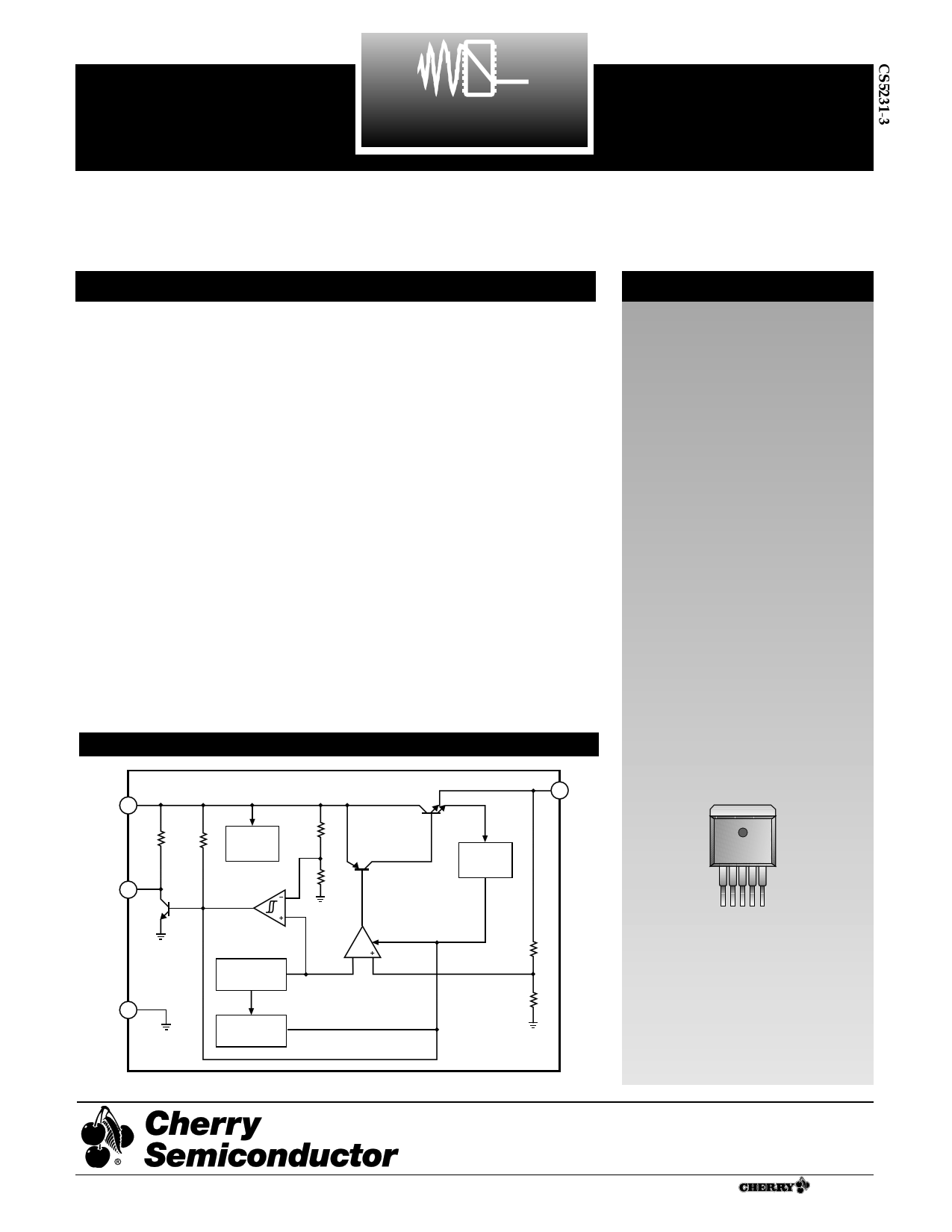
Block Diagram
VOUT
VIN
Linear Regulator
s 3.3V ± 2% Output Voltage
s 3mA Quiescent Current
@ 500mA
s Fast Transient Response
s Current Limit
s Thermal Shutdown with
Hysteresis
s 450µA Reverse Output
Current
s Fast Transient Response
System Power Management
s Auxiliary Supply Control
Package Options
5 Lead D2PAK
10kΩ 50kΩ
Internal
Bias
AuxDrv
Gnd
−
VIN UV +
Comparator
Bandgap
Reference
Thermal
Shutdown
Current
Limit
Error
Amp
VREF
−
Shutdown
1
1. No Connect
2. VIN
3. Gnd
4. VOUT
5. AuxDrv
Tab = Gnd
Consult factory for other package
options.
Rev. 3/31/99
Cherry Semiconductor Corporation
2000 South County Trail, East Greenwich, RI 02818
Tel: (401)885-3600 Fax: (401)885-5786
Email: [email protected]
Web Site: www.cherry-semi.com
1 A ® Company
1 page 
Application Circuit
+5V PCI
C1
33µF
VIN VOUT
CS5231-3
Gnd AuxDrv
+3.3V VAUX
C1
33µF
M1 ASIC
C3
33µF
VDD
*indicates PFET body diode
Application Information
Theory of Operation
The CS5231-3 is a fixed 3.3V linear regulator that contains
an auxiliary drive control feature. When VIN is greater than
the typical 4.5V threshold, the IC functions as a linear regu-
lator. It provides up to 500mA of current to a load through
a composite PNP-NPN pass transistor. An output capacitor
greater than 10µF with equivalent series resistance less
than 1Ω is required for compensation. More information is
provided in the Stability Considerations section.
The CS5231-3 provides an auxiliary drive feature that
allows a load to remain powered even if the VIN supply for
the IC is absent. An external p-channel FET is the only
additional component required to implement this function
if an auxiliary power supply is available. The PFET gate is
connected to the AuxDrv lead. The PFET drain is connect-
ed to the auxiliary power supply, and the PFET source is
connected to the load. The polarity of this connection is
very important, since the PFET body diode will be connect-
ed between the load and the auxiliary supply. If the PFET
is connected with its drain to the load and its source to the
supply, the body diode will be forward-biased if the auxil-
iary supply is turned off. This will result in the linear regu-
lator providing current to everything on the auxiliary sup-
ply rail.
The AuxDrv lead is internally connected to a 10kΩ resistor
and to a saturating NPN transistor that acts as a switch. If
the VIN supply is off, the AuxDrv output will connect the
PFET gate to ground through the 10kΩ resistor, and the
PFET will conduct current to the load.
As the VIN supply begins to rise, the AuxDrv lead will also
rise until it reaches a typical voltage of about 650mV. The
NPN transistor connected to the AuxDrv lead will saturate
at this point, and the gate of the PFET will be pulled down
to a typical voltage of about 100mV. The PFET will contin-
ues to conduct current to the load.
The VIN supply voltage will continue to rise, but the linear
regulator output is disabled until VIN reaches a typical
threshold of 4.5V. During this time, the load continues to
be powered by the auxiliary driver. Once the 4.5V VIN
threshold is reached, the saturating NPN connected to the
AuxDrv lead turns off. The on-chip 10kΩ pull-up resistor
will pull the PFET gate up to VIN, thus turning the PFET
off. The linear regulator turns on at the same time. An
external compensation capacitor is required for the linear
regulator to be stable, and this capacitance also serves as a
charge reservoir to minimize any “glitching” that might
result during the supply changeover. Hysteresis is present
in the AuxDrv circuitry, requiring VIN to drop by 100mV
(typical) after the linear regulator is providing power to the
load before the AuxDrv circuitry can be re-enabled.
VIN
VOUT
VAUXDRV
IOUT = STARTUP 375mA
Figure 1. Initial power-up, VAUX not present ROUT = 8.8Ω.
VIN
VOUT
VAUXDRV
IOUT = 375mA VAUX = 3.30V
Figure 2a. Power-up, VAUX = 3.30V. Note the “oscillatory performance”
as the linear regulator charges the VOUT node. IOUT × RDS(ON) ≈ 130mV
5
5 Page 
Package Specification
PACKAGE DIMENSIONS IN mm (INCHES)
PACKAGE THERMAL DATA
Thermal Data
5Lead
D2PAK
RΘJC
typ
2.5
˚C/W
RΘJA
typ
10-50*
˚C/W
*Depending on thermal properties of substrate. RΘJA = RΘJC + RΘCA
5 Lead D2PAK (DP)
10.31 (.406)
10.05 (.396)
1.68 (.066)
1.40 (.055)
1.40 (.055)
1.14 (.045)
8.53 (.336)
8.28 (.326)
15.75 (.620)
14.73 (.580)
1.70 (.067) REF
0.91 (.036)
0.66 (.026)
.254 (.010) REF
2.74(.108)
2.49(.098)
2.79 (.110)
2.29 (.090)
4.57 (.180)
4.31 (.170)
0.10 (.004)
0.00 (.000)
Ordering Information
Part Number
CS5231-3GDP5
CS5231-3GDPR5
Description
5 Lead D2PAK
5 Lead D2PAK (tape & reel)
Rev. 3/31/99
Cherry Semiconductor Corporation reserves the right to
make changes to the specifications without notice. Please
contact Cherry Semiconductor Corporation for the latest
available information.
11 © 1999 Cherry Semiconductor Corporation
11 Page | ||
| Páginas | Total 11 Páginas | |
| PDF Descargar | [ Datasheet CS5231-3GDPR5.PDF ] | |
Hoja de datos destacado
| Número de pieza | Descripción | Fabricantes |
| CS5231-3GDPR5 | 500mA/ 3.3V Linear Regulator with Auxiliary Control | Cherry Semiconductor Corporation |
| Número de pieza | Descripción | Fabricantes |
| SLA6805M | High Voltage 3 phase Motor Driver IC. |
Sanken |
| SDC1742 | 12- and 14-Bit Hybrid Synchro / Resolver-to-Digital Converters. |
Analog Devices |
|
DataSheet.es es una pagina web que funciona como un repositorio de manuales o hoja de datos de muchos de los productos más populares, |
| DataSheet.es | 2020 | Privacy Policy | Contacto | Buscar |