|
|
PDF CS5339-KS Data sheet ( Hoja de datos )
| Número de pieza | CS5339-KS | |
| Descripción | 16-Bit/ Stereo A/D Converters for Digital Audio | |
| Fabricantes | ETC | |
| Logotipo |  |
|
Hay una vista previa y un enlace de descarga de CS5339-KS (archivo pdf) en la parte inferior de esta página. Total 30 Páginas | ||
|
No Preview Available !
Semiconductor Corporation
CS5336 CS5338 CS5339
16-Bit, Stereo A/D Converters for Digital Audio
Features
• Complete CMOS Stereo A/D System
Delta-Sigma A/D Converters
Digital Anti-Alias Filtering
S/H Circuitry and Voltage Reference
• Adjustable System Sampling Rates
including 32kHz, 44.1 kHz & 48kHz
• Low Noise and Distortion
>90 dB S/(N+D)
• Internal 64X Oversampling
• Linear Phase Digital Anti-Alias Filtering
0.01dB Passband Ripple
80dB Stopband Rejection
• Low Power Dissipation: 400 mW
Power-Down Mode for Portable
Applications
• Evaluation Board Available
General Description
The CS5336, CS5338 & CS5339 are complete analog-
to-digital converters for stereo digital audio systems.
They perform sampling, analog-to-digital conversion and
anti-aliasing filtering, generating 16-bit values for both
left and right inputs in serial form. The output word rate
can be up to 50 kHz per channel.
The ADCs use delta-sigma modulation with 64X over-
sampling, followed by digital filtering and decimation,
which removes the need for an external anti-alias filter.
The CS5336 & CS5338 have an SCLK which clocks out
data on rising edges. The CS5339 has an SCLK which
clocks out data on falling edges.
The CS5336 has a filter passband of dc to 22kHz. The
CS5338 & CS5339 have a filter passband of dc to 24
kHz. The filters have linear phase, 0.01 dB passband
ripple, and >80 dB stopband rejection.
The ADC’s are housed in a 0.6" wide 28-pin plastic DIP,
and also in a 0.3" wide 28-pin SOIC surface mount
package. Extended temperature range versions of the
CS5336 are also available.
ORDERING INFORMATION: See Page 3-59
28
VREF
ICLKA APD ACAL
23 6
7
Voltage Reference
A IN L
ZEROL
2
3
S/H
AIN R
ZEROR
27
26
AGND 1
S /H
LP Filter
Com parator
DAC
LP Filter
Com parator
DAC
O C LKD ICLKD FSYN C SCLK L/R
21 20
1 7 15 14
S erial O utput Interface
16
12 S D A T A
13
CMODE
SMODE
Digital Decimation
Filter
11
TST
Digital Decim ation
Filter
C a lib ra tio n
Microcontroller
8
C a lib ra tio n
NC
SRAM
22
NC
45
VA+ VA-
25 24
VL+ LGND
9 10
DCAL DPD
18 19
VD+ DGND
Crystal Semiconductor Corporation
P.O. Box 17847, Austin, TX 78760
(512) 445-7222 FAX: (512) 445-7581
AUG ’93
DS23F1
3-39
1 page 
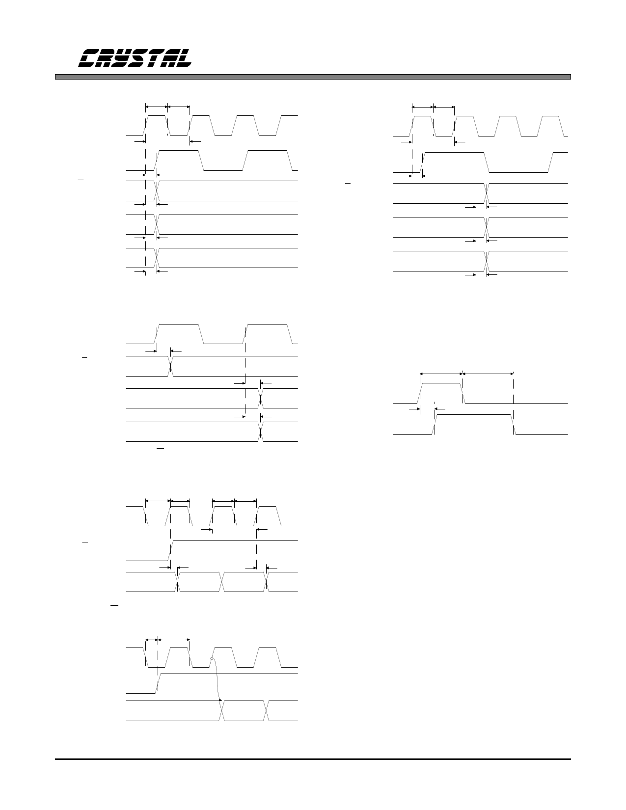
t clkh t clkl
ICLKD
OCLKD
(CMODE low)
L/R output
(MASTER mode)
FSYNC output
(MASTER mode)
SCLK output
(MASTER mode)
t clkw1
t io1
t ilr1
t ifs1
t isclk1
ICLKD to Outputs Propagation Delays (CMODE low)
SCLK output
(MASTER mode)
t mslr
L/ R output
(MASTER mode)
SDATA
FSYNC output
(MASTER mode)
t sdo
t msfs
SCLK to SDATA, L/R & FSYNC - MASTER Mode
CS5336, CS5338, CS5339
t clkh2 t clkl2
ICLKD
OCLKD
(CMODE high)
L/R output
(MASTER mode)
FSYNC output
(MASTER mode)
SCLK output
(MASTER mode)
t clkw2
t io2
t ilr2
t ifs2
t isclk2
ICLKD to Outputs Propagation Delays (CMODE high)
t pdw
t pcf
DPD
DCAL
t pcr
Power Down & Calibration Timing
SCLK input
(SLAVE mode)
L/R input
(SLAVE mode)
SDATA
t slr1 t slr2
t sclkh t sclkl
t lrdss
MSB
t sclkw
MSB-1
t dss
MSB-2
SCLK to L/R & SDATA - SLAVE mode, FSYNC high
SCLK input
(SLAVE mode)
FSYNC input
(SLAVE mode)
t sfs1
t sfs2
SDATA
MSB
MSB-1
MSB-2
FSYNC to SCLK - SLAVE Mode, FSYNC Controlled.
DS23F1
3-43
5 Page 
CS5336, CS5338, CS5339
greater than 10 µF, as stated in the "Power-Up
Considerations" section.
During the offset calibration cycle, the digital sec-
tion of the part measures and stores the value of
the calibration input of each channel in registers.
The calibration input value is subtracted from all
future outputs. The calibration input may be ob-
tained from either the analog input pins (AINL
and AINR) or the zero pins (ZEROL and
ZEROR) depending on the state of the ACAL pin.
With ACAL low, the analog input pin voltages are
measured, and with ACAL high, the zero pin volt-
ages are measured.
As shown in Figure 6, the DCAL output is high
during calibration, which takes 4096 L/R clock
cycles. If DCAL is connected to the ACAL input,
the calibration routine will measure the voltage on
ZEROR and ZEROL. These should be connected
directly to ground or through a network matched
to that present on the analog input pins. Internal
offsets of each channel will thus be measured and
subsequently subtracted.
Alternatively, ACAL may be permanently con-
nected low and DCAL utilized to control a
multiplexer which grounds the user’s front end.
In this case, the calibration routine will measure
and store not only the internal offsets but also
any offsets present in the front end input circuitry.
During calibration, the digital output of both
channels is forced to a 2’s complement zero. Sub-
traction of the calibration input from conversions
after calibration substantially reduces any
power on click that might otherwise be experi-
enced. A short delay of approximately 40 output
words will occur following calibration for the
digital filter to begin accurately tracking audio
band signals.
Power-up Considerations
Upon initial application of power to the supply
pins, the data in the calibration registers will be
indeterminate. A calibration cycle should always
be initiated after application of power to replace
potentially large values of data in these registers
with the correct values.
The modulators settle very quickly (a matter of
microseconds) after the analog section is powered
on, either through the application of power, or by
exiting the power-down mode. The voltage refer-
ence can take a much longer time to reach a final
value due to the presence of large external capaci-
tance on the VREF pin; allow approximately
5 ms/µF. The calibration period is long enough to
allow the reference to settle for capacitor values of
up to 10 µF. If a larger capacitor is used, addi-
tional time between APD going low and DPD
going low should be allowed for VREF settling
before a calibration cycle is initiated.
Grounding and Power Supply Decoupling
As with any high resolution converter, the ADC
requires careful attention to power supply and
grounding arrangements if its potential perform-
ance is to be realized. Figure 1 shows the
recommended power arrangements, with VA+,
VA- and VL+ connected to a clean ± 5 V supply.
VD+, which powers the digital filter, may be run
from the system +5V logic supply, provided that
it is not excessively noisy (< ± 50 mV pk-to-pk).
Alternatively, VD+ may be powered from VA+ via
a ferrite bead. In this case, no additional devices
should be powered from VD+. Analog ground and
digital ground should be connected together near
to where the supplies are brought onto the printed
circuit board. Decoupling capacitors should be as
near to the ADC as possible, with the low value
ceramic capacitor being the nearest.
The printed circuit board layout should have sepa-
rate analog and digital regions and ground planes,
DS23F1
3-49
11 Page | ||
| Páginas | Total 30 Páginas | |
| PDF Descargar | [ Datasheet CS5339-KS.PDF ] | |
Hoja de datos destacado
| Número de pieza | Descripción | Fabricantes |
| CS5339-KP | 16-Bit/ Stereo A/D Converters for Digital Audio | ETC |
| CS5339-KS | 16-Bit/ Stereo A/D Converters for Digital Audio | ETC |
| Número de pieza | Descripción | Fabricantes |
| SLA6805M | High Voltage 3 phase Motor Driver IC. |
Sanken |
| SDC1742 | 12- and 14-Bit Hybrid Synchro / Resolver-to-Digital Converters. |
Analog Devices |
|
DataSheet.es es una pagina web que funciona como un repositorio de manuales o hoja de datos de muchos de los productos más populares, |
| DataSheet.es | 2020 | Privacy Policy | Contacto | Buscar |
