|
|
|
PDF CS5651GDWR16 Data sheet ( Hoja de datos )
| Número de pieza | CS5651GDWR16 | |
| Descripción | High Performance Dual Channel Current Mode Controller with ENABLE | |
| Fabricantes | Cherry Semiconductor Corporation | |
| Logotipo | ||
Hay una vista previa y un enlace de descarga de CS5651GDWR16 (archivo pdf) en la parte inferior de esta página. Total 8 Páginas | ||
|
No Preview Available !
CS5651
High Performance Dual Channel
Current Mode Controller with ENABLE
Description
Features
The CS5651 is a high performance,
fixed frequency, dual current mode
controller specifically designed for
Off-Line and DC to DC converter
applications. It offers the designer a
cost effective solution with minimal
external components. This integrat-
ed circuit features a unique oscilla-
tor for precise duty cycle limit and
frequency control, a temperature
compensated reference, two high
gain error amplifiers, two current
sensing comparators, and two high
current totem pole outputs ideally
suited for driving power MOSFETs.
One of the outputs, VOUT2 is switch-
able via the ENABLE2 pin.
Also included are protective fea-
tures consisting of input and refer-
ence undervoltage lockouts, each
with hysteresis; cycle-by-cycle cur-
rent limiting; and a latch for single
pulse metering of each output.
The CS5651 is pin compatible with
the MC34065H.
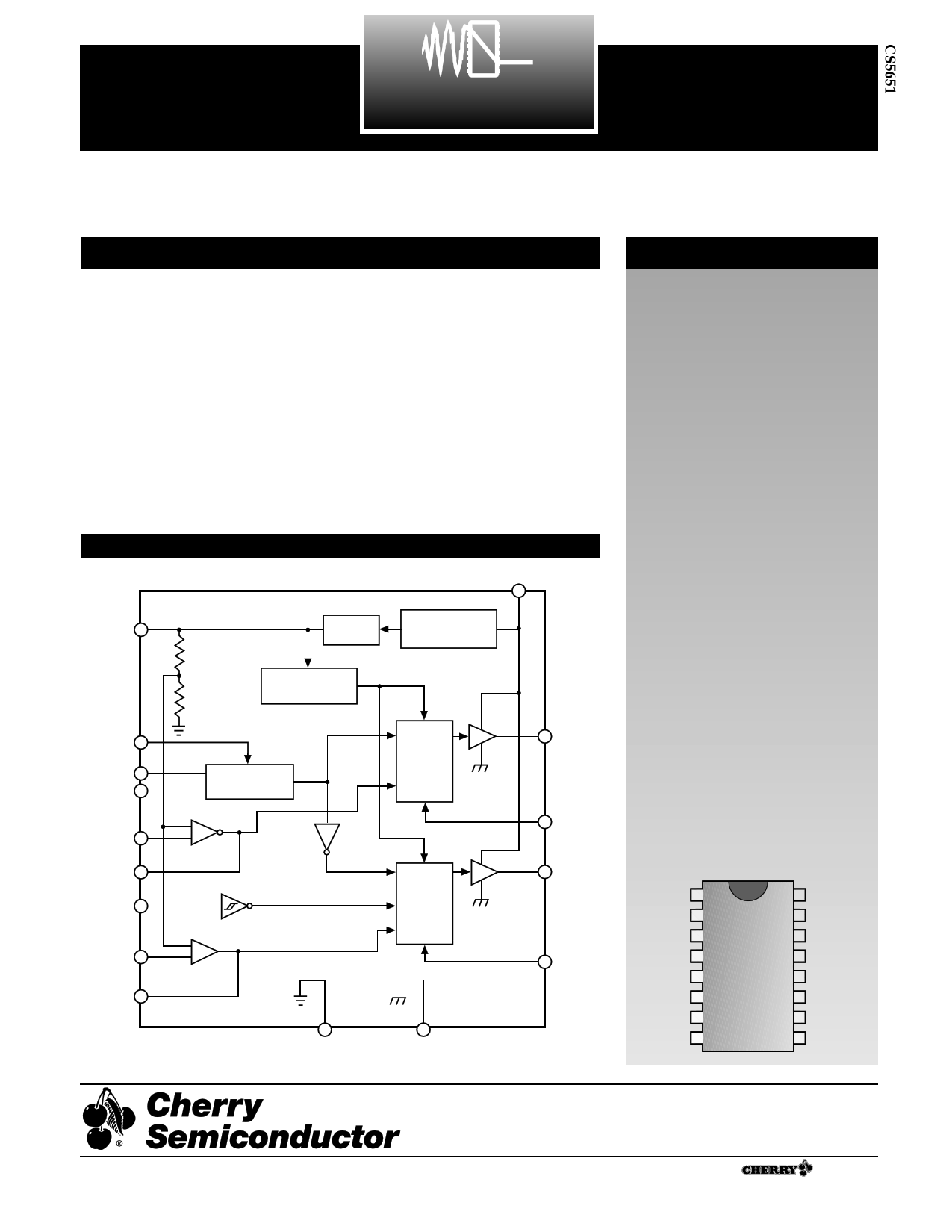
Block Diagram
VCC
VREF
5.0V Ref
VREF
Undervoltage
Lockout
VCC
Undervoltage
Lockout
s Oscillator has Precise
Duty Cycle
Limit and Frequency
Control
s 500kHz Current Mode
Operation
s Automatic Feed Forward
Compensation
s Separate Latching PWMs
for Cycle-By-Cycle
Current Limiting
s Internally Trimmed
Reference with
Undervoltage Lockout
s Switchable Second
Output
s Two High Current Totem
Pole Outputs
s Input Undervoltage
Lockout with Hysteresis
SYNC
CT
RT
VFB1
COMP1
ENABLE2
VFB2
COMP2
Oscillator
+
-
Error
Amp 1
+
-
Error
Amp 2
Gnd
Latching
PWM 1
Latching
PWM 2
Pwr Gnd
VOUT1
Sense1
VOUT2
Sense2
Package Options
16L PDIP & SO Wide
SYNC 1
CT 2
RT 3
VFB1 4
COMP1 5
SENSE1 6
VOUT1 7
Gnd 8
16 VCC
15 VREF
14 ENABLE2
13 VFB2
12 COMP2
11 Sense2
10 VOUT2
9 Pwr Gnd
Rev. 3/9/99
Cherry Semiconductor Corporation
2000 South County Trail, East Greenwich, RI 02818
Tel: (401)885-3600 Fax: (401)885-5786
Email: [email protected]
Web Site: www.cherry-semi.com
1
A Company
®
1 page 
Typical Performance Characteristics: continued
Reference Voltage Change vs. Source Current
0
VCC = 15V
-4.0
Reference Short Circuit Current vs. Temperature
120
-8.0
TA = –55°C
-12
TA =
-16 25°C
TA = 125°C
-20
-24
0 20 40 60 80 100 120
I ref, REFERENCE SOURCE CURRENT (mA)
Output Saturation Voltage vs. Load Current
0
VCC
-1.0
-2.0
SOURCE SATURATION
(LOAD TO GROUND)
VCC=15V
80µS PULSED LOAD
120Hz RATE
TA=25°C
TA= –55°C
2.0
1.0
0
0
TA= –55°C
TA=25°C
GND
SINK
SATURATION
(LOAD TO VCC)
200 400 600 800
OUTPUT LOAD CURRENT (mA)
100
80
60-55 -25 0 25 50 75 100
TA, AMBIENT TEMPERATURE (°C)
Supply Current vs. Supply Voltage
125
32
RT=8.2kΩ
CT=3.3nF
24 VFB 1, 2=0V
CURRENT SENSE 1, 2=0V
TA=25°C
16
8.0
0
0 4.0 8.0 12 16 20
VCC, SUPPLY VOLTAGE (V) - CS-5651
Operating Description
The CS5651 is a high performance, fixed frequency, dual
channel current mode PWM controller for Off-Line and
DC to DC converter applications. Each channel contains a
high gain error amplifier, current sensing comparator,
pulse width modulator latch, and totem pole output driv-
er. The oscillator, reference, and undervoltage lockout cir-
cuits are common to both channels.
Oscillator
The oscillator has both precise frequency and duty cycle
control. The oscillator frequency is programmed by the
timing components RT and CT. Capacitor CT is charged
and discharged by an equal magnitude internal current
source and sink, that generates a symmetrical 50 percent
duty cycle waveform at CT. The oscillator peak and valley
thresholds are 3.5V and 1.6V respectively. The source/
sink current is controlled by resistor RT. For proper opera-
tion over temperature range RT’s value should be between
4.0kΩ to 16kΩ.
As CT charges and discharges, an internal blanking pulse
is generated that alternately drives the inputs of the upper
and lower NOR gates high. This, in conjunction with a
precise amount of delay time introduced into each chan-
nel, produces well defined non-overlapping output duty
cycles. Output 2 is enabled while CT is charging, and
Output 1 is enabled during the discharge. Even at 500kHz,
each output is capable of approximately 44% duty cycle,
making this controller suitable for high frequency power
conversion applications.
In noise sensitive applications it may be necessary to syn-
chronize the converter with an external system clock. This
can be accomplished by applying an external clock signal.
For reliable synchronization, the oscillator frequency
should be set about 10% slower than the clock frequency.
The rising edge of the clock signal applied to SYNC, termi-
nates the charging of CT and VOUT2 conduction. By tailor-
ing the clock waveform symmetry, accurate duty cycle
clamping of either output can be achieved.
Error Amplifier
Each channel contains a fully-compensated error amplifier
with access to the output and inverting input. The amplifi-
er features a typical dc voltage gain of 100 dB, and a unity
gain bandwidth of 1.0 MHz with 71 degrees of phase mar-
gin. The non-inverting input is internally biased at 2.5V.
The converter output voltage is typically divided down
and monitored by the inverting input through a resistor
divider. The maximum input bias current is -1.0 µA which
will cause an output voltage error that is equal to the
product of the input bias current and the equivalent input
divider resistance.
Its output voltage is offset by two diode drops (≈1.4V) and
divided by three before it connects to the inverting input
of the current sense comparator. This guarantees that both
5
5 Page | ||
| Páginas | Total 8 Páginas | |
| PDF Descargar | [ Datasheet CS5651GDWR16.PDF ] | |
Hoja de datos destacado
| Número de pieza | Descripción | Fabricantes |
| CS5651GDWR16 | High Performance Dual Channel Current Mode Controller with ENABLE | Cherry Semiconductor Corporation |
| Número de pieza | Descripción | Fabricantes |
| SLA6805M | High Voltage 3 phase Motor Driver IC. |
Sanken |
| SDC1742 | 12- and 14-Bit Hybrid Synchro / Resolver-to-Digital Converters. |
Analog Devices |
|
DataSheet.es es una pagina web que funciona como un repositorio de manuales o hoja de datos de muchos de los productos más populares, |
| DataSheet.es | 2020 | Privacy Policy | Contacto | Buscar |