|
|
PDF AD9886 Data sheet ( Hoja de datos )
| Número de pieza | AD9886 | |
| Descripción | Analog Interface for Flat Panel Displays | |
| Fabricantes | Analog Devices | |
| Logotipo |  |
|
Hay una vista previa y un enlace de descarga de AD9886 (archivo pdf) en la parte inferior de esta página. Total 30 Páginas | ||
|
No Preview Available !
a
FEATURES
Analog Interface
140 MSPS Maximum Conversion Rate
330 MHz Analog Bandwidth
0.5 V to 1.0 V Analog Input Range
500 ps p-p PLL Clock Jitter at 140 MSPS
3.3 V Power Supply
Full Sync Processing
Midscale Clamp for YUV Applications
GENERAL DESCRIPTION
The AD9886 is a complete 8-bit 140 MSPS monolithic analog
interface optimized for capturing RGB graphics signals from
personal computers and workstations. Its 140 MSPS encode
rate capability and full-power analog bandwidth of 330 MHz
supports resolutions up to SXGA (1280 × 1024 at 75 Hz).
For ease of design and to minimize cost, the AD9886 is a fully
integrated interface solution for FPDs. The AD9886 includes a
140 MHz triple ADC with internal 1.25 V reference, PLL to
generate a pixel clock from an HSYNC, and programmable
gain, offset, and clamp control. The user provides only a 3.3 V
power supply, analog input, and an HSYNC signal. Three-state
CMOS outputs may be powered from 2.5 V to 3.3 V.
The AD9886’s on-chip PLL generates a pixel clock from an
HSYNC. Pixel clock output frequencies range from 12 MHz to
140 MHz. PLL clock jitter is 500 ps p-p typical at 140 MSPS.
When the COAST signal is presented, the PLL maintains its
output frequency in the absence of HSYNC. A sampling phase
adjustment is provided. Data, HSYNC and Clock output phase
relationships are maintained. The PLL can be disabled and an
external clock input provided as the pixel clock. The AD9886
also offers full sync processing for composite sync and sync-on-
green applications.
A clamp signal is generated internally or may be provided by the
user through the CLAMP input pin. This interface is fully pro-
grammable via a 2-wire serial interface.
Analog Interface for
Flat Panel Displays
AD9886
FUNCTIONAL BLOCK DIAGRAM
ANALOG INTERFACE
RIN CLAMP
A/D
AD9886
8
8
8
GIN CLAMP
8
A/D
8
8
BIN CLAMP
8
A/D
8
8
ROUTA
ROUTB
GOUTA
GOUTB
BOUTA
BOUTB
HSYNC
COAST
CLAMP
CKINV
CKEXT
FILT
SYNC
PROCESSING
AND CLOCK
GENERATION
SCL
SDA
A1
A0
SERIAL REGISTER AND
POWER MANAGEMENT
2
REF
DATACK
HSOUT
VSOUT
SOGOUT
REFOUT
REFIN
REV. 0
Information furnished by Analog Devices is believed to be accurate and
reliable. However, no responsibility is assumed by Analog Devices for its
use, nor for any infringements of patents or other rights of third parties
which may result from its use. No license is granted by implication or
otherwise under any patent or patent rights of Analog Devices.
One Technology Way, P.O. Box 9106, Norwood, MA 02062-9106, U.S.A.
Tel: 781/329-4700 World Wide Web Site: http://www.analog.com
Fax: 781/326-8703
© Analog Devices, Inc., 2001
1 page 
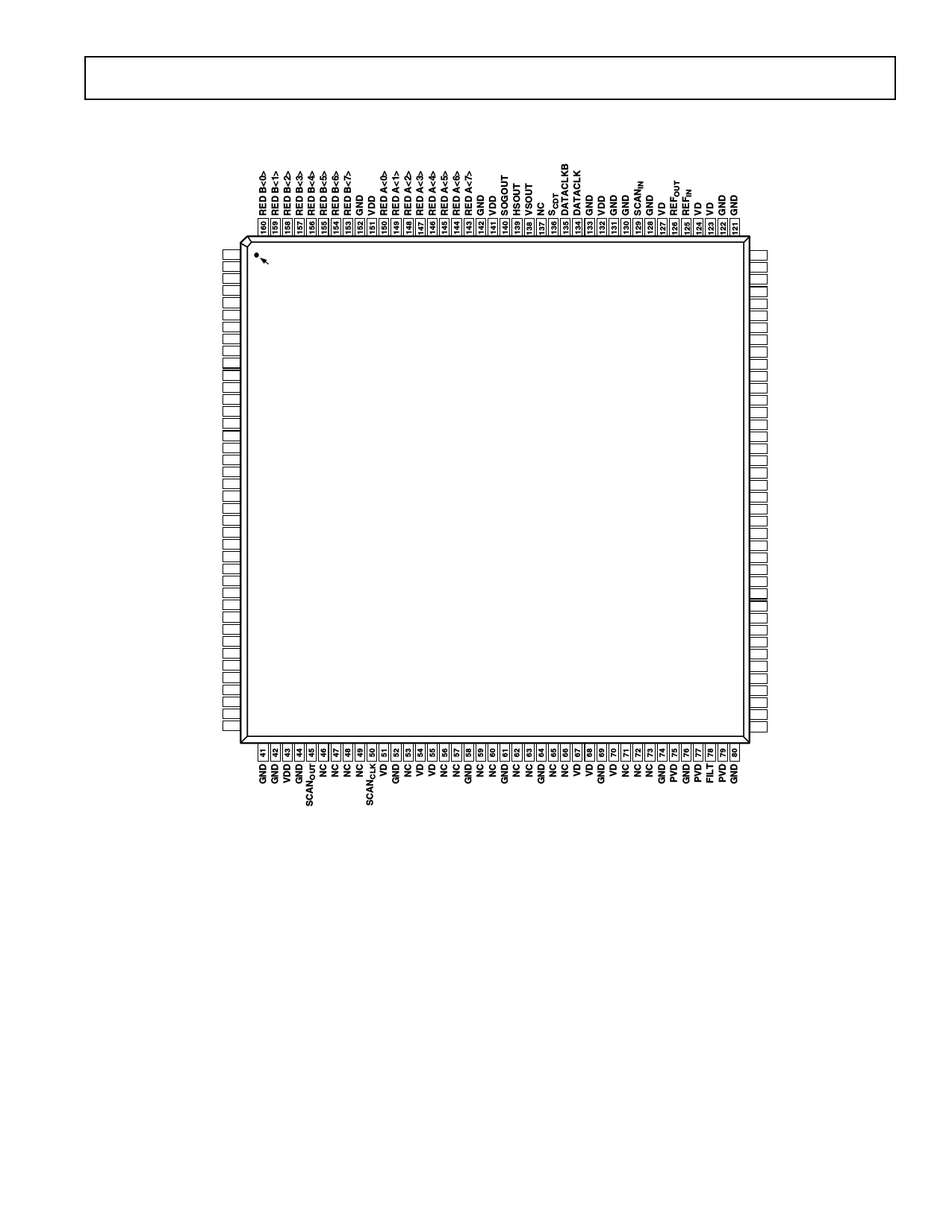
PIN CONFIGURATION
VDD 1
GND 2
GREEN A<7> 3
GREEN A<6> 4
GREEN A<5> 5
GREEN A<4> 6
GREEN A<3> 7
GREEN A<2> 8
GREEN A<1> 9
GREEN A<0> 10
VDD 11
GND 12
GREEN B<7> 13
GREEN B<6> 14
GREEN B<5> 15
GREEN B<4> 16
GREEN B<3> 17
GREEN B<2> 18
GREEN B<1> 19
GREEN B<0> 20
VDD 21
GND 22
BLUE A<7> 23
BLUE A<6> 24
BLUE A<5> 25
BLUE A<4> 26
BLUE A<3> 27
BLUE A<2> 28
BLUE A<1> 29
BLUE A<0> 30
VDD 31
GND 32
BLUE B<7> 33
BLUE B<6> 34
BLUE B<5> 35
BLUE B<4> 36
BLUE B<3> 37
BLUE B<2> 38
BLUE B<1> 39
BLUE B<0> 40
PIN 1
IDENTIFIER
NC = NO CONNECT
AD9886
TOP VIEW
(Not to Scale)
AD9886
120 RMIDSCV
119 RAIN
118 RCLAMPV
117 VD
116 GND
115 VD
114 VD
113 GND
112 GND
111 GMIDSCV
110 GAIN
109 GCLAMPV
108 SOGIN
107 VD
106 GND
105 VD
104 VD
103 GND
102 GND
101 BMIDSCV
100 BAIN
99 BCLAMPV
98 VD
97 GND
96 VD
95 GND
94 CKINV
93 CLAMP
92 SDA
91 SCL
90 A0
89 A1
88 PVD
87 PVD
86 GND
85 GND
84 COAST
83 CKEXT
82 HSYNC
81 VSYNC
REV. 0
–5–
5 Page 
AD9886
The clamp timing can be established by simply exercising the
CLAMP pin at the appropriate time (with EXTCLMP = 1).
The polarity of this signal is set by the Clamp Polarity bit.
A simpler method of clamp timing employs the AD9886 inter-
nal clamp timing generator. The Clamp Placement register is
programmed with the number of pixel times that should pass
after the trailing edge of HSYNC before clamping starts. A
second register (Clamp Duration) sets the duration of the
clamp. These are both 8-bit values, providing considerable
flexibility in clamp generation. The clamp timing is referenced
to the trailing edge of HSYNC because, although HSYNC
duration can vary widely, the back porch (black reference)
always follows HSYNC. A good starting point for establishing
clamping is to set the clamp placement to 08h (providing eight
pixel periods for the graphics signal to stabilize after sync) and
set the clamp duration to 14h (giving the clamp 20 pixel periods
to reestablish the black reference).
Clamping is accomplished by placing an appropriate charge on
the external input coupling capacitor. The value of this capaci-
tor affects the performance of the clamp. If it is too small, there
will be a significant amplitude change during a horizontal line
time (between clamping intervals). If the capacitor is too large,
it will take excessively long for the clamp to recover from a large
change in incoming signal offset. The recommended value
(47 nF) results in recovering from a step error of 100 mV to
within 1/2 LSB in 10 lines with a clamp duration of 20 pixel
periods on a 60 Hz SXGA signal.
YUV Clamping
YUV graphic signals are slightly different from RGB signals in
that the dc reference level (black level in RGB signals) can be at
the midpoint of the video signal rather than the bottom. For
these signals it can be necessary to clamp to the midscale range
of the A/D converter range (10h) rather than bottom of the A/D
converter range (00h).
Clamping to midscale rather than ground can be accomplished
by setting the clamp select bits in the series bus register. Each of
the three converters has its own selection bit so that they can be
clamped to either midscale or ground independently. These bits
are located in Register 0Fh and are Bits 0–2.
The midscale reference voltage that each A/D converter clamps
to is provided independently on the RMIDSCV, GMIDSCV, and
BMIDSCV pins. Each converter must have its own midscale refer-
ence because both offset adjustment and gain adjustment for
each converter will affect the dc level of midscale.
During clamping, each A/D converter is clamped to its respec-
tive midscale reference input. These inputs are pins RCLAMPV,
GCLAMPV, and BCLAMPV for the red, green, and blue converters
respectively. The typical connections for both RGB and YUV
clamping are shown below in Figure 2. Note: if midscale clamp-
ing is not required, all of the midscale voltage outputs should
still be connected to ground through a 0.1 µF capacitor.
0.1F
0.1F
0.1F
RMIDSCV
RCLAMPV
GMIDSCV
GCLAMPV
BMIDSCV
BCLAMPV
Figure 2. Typical Clamp Configuration for RBG/YUV
Applications
Gain and Offset Control
The AD9886 can accommodate input signals with inputs rang-
ing from 0.5 V to 1.0 V full scale. The full-scale range is set in
three 8-bit registers (Red Gain, Green Gain, and Blue Gain).
Note that increasing the gain setting results in an image with
less contrast.
The offset control shifts the entire input range, resulting in a
change in image brightness. Three 7-bit registers (Red Offset,
Green Offset, Blue Offset) provide independent settings for
each channel.
The offset controls provide a ± 63 LSB adjustment range. This
range is connected with the full-scale range, so if the input range
is doubled (from 0.5 V to 1.0 V) then the offset step size is also
doubled (from 2 mV per step to 4 mV per step).
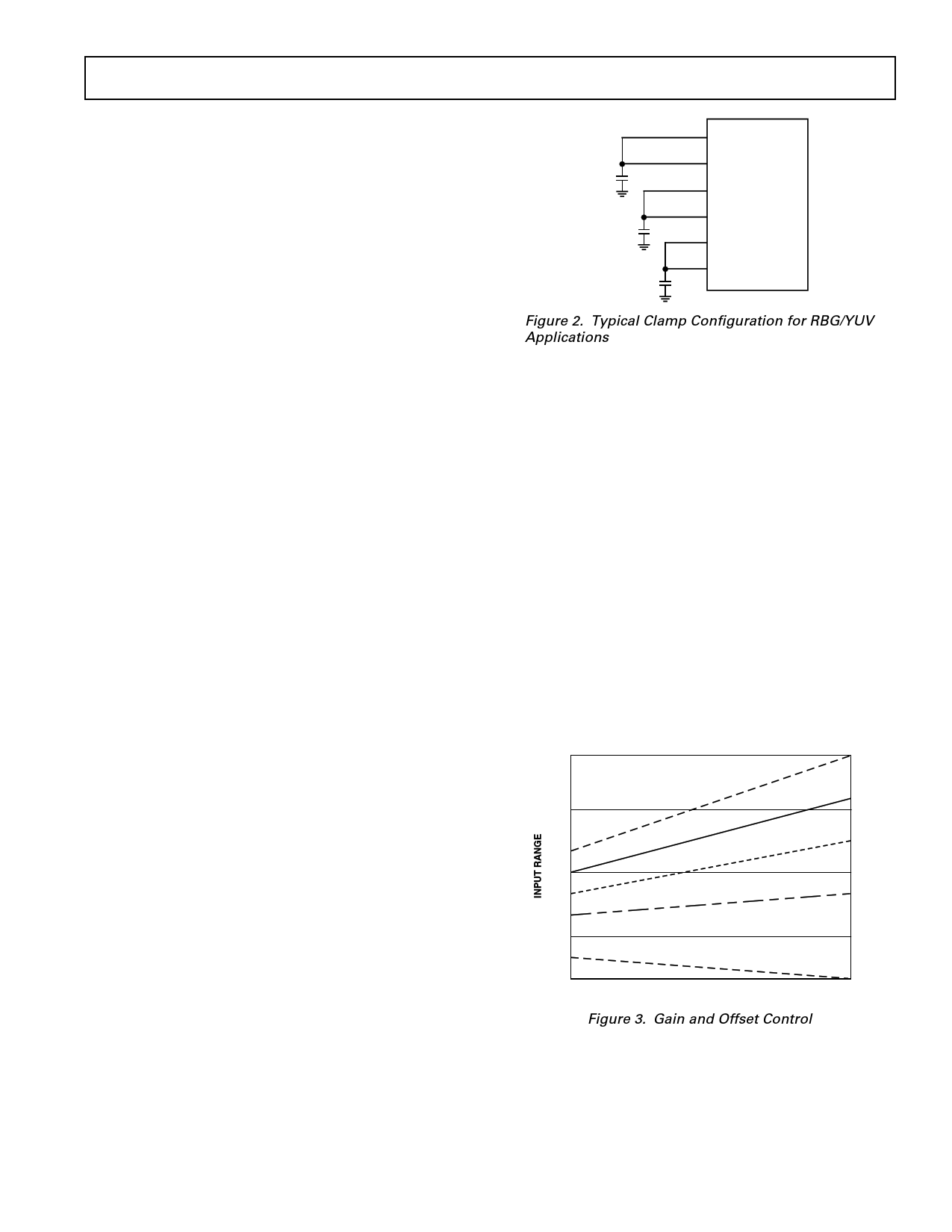
Figure 3 illustrates the interaction of gain and offset controls.
The magnitude of an LSB in offset adjustment is proportional
to the full-scale range, so changing the full-scale range also
changes the offset. The change is minimal if the offset setting is
near midscale. When changing the offset, the full-scale range is
not affected, but the full-scale level is shifted by the same amount
as the zero-scale level.
1.0V
OFFSET = 7Fh
OFFSET = 3Fh
OFFSET = 00h
0.5V
OFFSET = 7Fh
0.0V
OFFSET = 3Fh
OFFSET = 00h
00h
GAIN
Figure 3. Gain and Offset Control
FFh
REV. 0
–11–
11 Page | ||
| Páginas | Total 30 Páginas | |
| PDF Descargar | [ Datasheet AD9886.PDF ] | |
Hoja de datos destacado
| Número de pieza | Descripción | Fabricantes |
| AD9880 | Analog/HDMI Dual Display Interface | Analog Devices |
| AD9882 | Dual Interface for Flat Panel Displays | Analog Devices |
| AD9882A | Dual Interface | Analog Devices |
| AD9883 | 110 MSPS Analog Interface for Flat Panel Displays | Analog Devices |
| Número de pieza | Descripción | Fabricantes |
| SLA6805M | High Voltage 3 phase Motor Driver IC. |
Sanken |
| SDC1742 | 12- and 14-Bit Hybrid Synchro / Resolver-to-Digital Converters. |
Analog Devices |
|
DataSheet.es es una pagina web que funciona como un repositorio de manuales o hoja de datos de muchos de los productos más populares, |
| DataSheet.es | 2020 | Privacy Policy | Contacto | Buscar |
