|
|
|
PDF AD9895 Data sheet ( Hoja de datos )
| Número de pieza | AD9895 | |
| Descripción | CCD Signal Processors with Precision Timing Generator | |
| Fabricantes | Analog Devices | |
| Logotipo | ||
Hay una vista previa y un enlace de descarga de AD9895 (archivo pdf) en la parte inferior de esta página. Total 30 Páginas | ||
|
No Preview Available !
a
CCD Signal Processors with
Precision Timing™ Generator
AD9891/AD9895
FEATURES
AD9891: 10-Bit 20 MHz Version
AD9895: 12-Bit 30 MHz Version
Correlated Double Sampler (CDS)
4 ؎6 dB Pixel Gain Amplifier (PxGA®)
2 dB to 36 dB 10-Bit Variable Gain Amplifier (VGA)
10-Bit 20 MHz A/D Converter (AD9891)
12-Bit 30 MHz A/D Converter (AD9895)
Black Level Clamp with Variable Level Control
Complete On-Chip Timing Generator
Precision Timing Core with 1 ns Resolution
On-Chip 5 V Horizontal and RG Drivers
2-Phase and 4-Phase H-Clock Modes
4-Phase Vertical Transfer Clocks
Electronic and Mechanical Shutter Modes
On-Chip Driver for External Crystal
On-Chip Sync Generator with External Sync Option
64-Lead CSPBGA Package
APPLICATIONS
Digital Still Cameras
Digital Video Camcorders
Industrial Imaging
PRODUCT DESCRIPTION
The AD9891 and AD9895 are highly integrated CCD signal
processors for digital still camera applications. Both include a
complete analog front end with A/D conversion combined with
a full-function programmable timing generator. A Precision
Timing core allows adjustment of high speed clocks with 1 ns
resolution at 20 MHz operation and 700 ps resolution at 30
MHz operation.
The AD9891 is specified at pixel rates of up to 20 MHz, and
the AD9895 is specified at 30 MHz. The analog front end
includes black level clamping, CDS, PxGA, VGA, and a 10-Bit
or 12-Bit A/D converter. The timing generator provides all the
necessary CCD clocks: RG, H-clocks, V-clocks, sensor gate
pulses, substrate clock, and substrate bias control. Operation is
programmed using a 3-wire serial interface.
Packaged in a space-saving 64-lead CSPBGA, the AD9891 and
AD9895 are specified over an operating temperature range of
–20°C to +85°C.
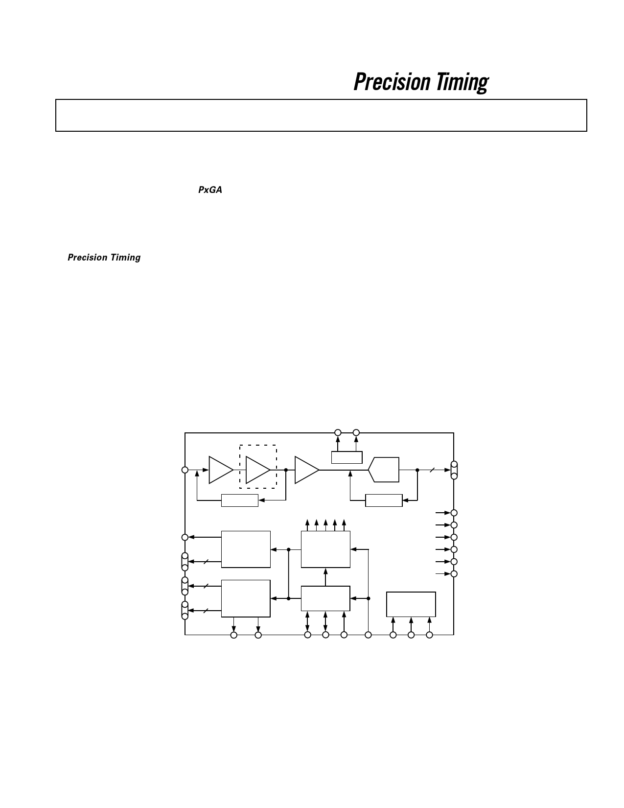
FUNCTIONAL BLOCK DIAGRAM
CCDIN
CDS
VRT VRB
4dB ؎ 6dB
PxGA
2dB TO 36dB
VGA
VREF
AD9891/AD9895
ADC
10 OR 12
DOUT
CLAMP
RG
H1–H4
V1–V4
VSG1–VSG8
HORIZONTAL
4 DRIVERS
4
V-H
8 CONTROL
INTERNAL CLOCKS
CLAMP
PRECISION
TIMING
GENERATOR
SYNC
GENERATOR
INTERNAL
REGISTERS
DCLK
CLPOB/PBLK
FD/LD
MSHUT
STROBE
CLO
VSUB SUBCK
HD VD SYNC CLI
SL SCK DATA
PxGA is a registered trademark and Precision Timing is a trademark of Analog Devices, Inc.
REV. A
Information furnished by Analog Devices is believed to be accurate and
reliable. However, no responsibility is assumed by Analog Devices for its
use, nor for any infringements of patents or other rights of third parties that
may result from its use. No license is granted by implication or otherwise
under any patent or patent rights of Analog Devices.
One Technology Way, P.O. Box 9106, Norwood, MA 02062-9106, U.S.A.
Tel: 781/329-4700
www.analog.com
Fax: 781/326-8703
© Analog Devices, Inc., 2002
1 page 
AD9891/AD9895
AD9895–ANALOG SPECIFICATIONS (AVDD1, AVDD2 = 3.0 V, fCLI = 30 MHz, TMIN to TMAX, unless otherwise noted.)
Parameter
Min Typ Max
Unit
Notes
CDS
Gain
Allowable CCD Reset Transient
Max Input Range before Saturation
Max CCD Black Pixel Amplitude
0
500
1.0
± 200
dB
mV
V p-p
mV
Input signal characteristics*
PIXEL GAIN AMPLIFIER (PxGA)
Max Input Range
Max Output Range
Gain Control Resolution
Gain Monotonicity
Gain Range
Min Gain (PxGA Code 32)
Med Gain (PxGA Code 0)
Max Gain (PxGA Code 31)
1.0
1.6
64
Guaranteed
–2.5
+3.5
+9.5
V p-p
V p-p
Steps
dB
dB Default setting
dB
VARIABLE GAIN AMPLIFIER (VGA)
Max Input Range
Max Output Range
Gain Control Resolution
Gain Monotonicity
Gain Range
Low Gain (VGA Code 70)
Max Gain (VGA Code 1023)
1.6
2.0
1024
Guaranteed
2
36
V p-p
V p-p
Steps
dB
dB
BLACK LEVEL CLAMP
Clamp Level Resolution
Clamp Level
Min Clamp Level
Max Clamp Level
256 Steps
Measured at ADC output
0 LSB
255 LSB
A/D CONVERTER
Resolution
Differential Nonlinearity (DNL)
No Missing Codes
Full-Scale Input Voltage
12
± 0.5 ± 1.0
Guaranteed
2.0
Bits
LSB
V
VOLTAGE REFERENCE
Reference Top Voltage (VRT)
2.0 V
Reference Bottom Voltage (VRB) 1.0 V
SYSTEM PERFORMANCE
Gain Accuracy
Low Gain (VGA Code 70)
567
Max Gain (VGA Code 1023)
38.5 39.5 40.5
Peak Nonlinearity, 500 mV Input Signal
0.2
Total Output Noise
0.8
Power Supply Rejection (PSR)
40
*Input signal characteristics defined as follows:
dB
dB
%
LSB rms
dB
Includes entire signal chain
Includes 4 dB default PxGA gain
Gain = (0.035 ϫ Code) + 3.55 dB
12 dB gain applied
AC grounded input, 6 dB gain applied
Measured with step change on supply
500mV TYP
RESET
TRANSIENT
200mV MAX
OPTICAL
BLACK PIXEL
1V MAX
INPUT
SIGNAL RANGE
Specifications subject to change without notice.
REV. A
–5–
5 Page 
AD9891/AD9895
SYSTEM OVERVIEW
Figure 5 shows the typical system block diagram for the AD9891/
AD9895 used in Master Mode. The CCD output is processed by
the AD9891/AD9895’s AFE circuitry, which consists of a CDS,
PxGA, VGA, black level clamp, and an A/D converter. The digi-
tized pixel information is sent to the digital image processor chip,
which performs the post-processing and compression. To operate
the CCD, all CCD timing parameters are programmed into the
AD9891/AD9895 from the system microprocessor, through the
3-wire serial interface. From the system master clock, CLI, pro-
vided by the image processor or external crystal, the AD9891/
AD9895 generates all of the CCD’s horizontal and vertical clocks
and all internal AFE clocks. External synchronization is provided
by a SYNC pulse from the microprocessor, which will reset
internal counters and resync the VD and HD outputs.
V-DRIVER
V1–V4, VSG1–VSG8, SUBCK
CCD
H1–H4, RG, VSUB
CCDIN
MSHUT
STROBE
AD989x
DOUT
DCLK
CLPOB/PBLK
LD/FD
HD, VD
CLI
SERIAL
INTERFACE
SYNC
P
DIGITAL
IMAGE
PROCESSING
ASIC
Figure 5. Typical System Block Diagram, Master Mode
Alternatively, the AD9891/AD9895 may be operated in Slave
Mode, in which the VD and HD are provided externally from
the image processor. In this mode, all AD9891/AD9895 timing
will be synchronized with VD and HD.
The H-drivers for H1–H4 and RG are included in the AD9891/
AD9895, allowing these clocks to be directly connected to the CCD.
H-drive voltage of up to 5 V is supported. An external V-driver is
required for the vertical transfer clocks, the sensor gate pulses,
and the substrate clock.
The AD9891/AD9895 also includes programmable MSHUT
and STROBE outputs, which may be used to trigger mechani-
cal shutter and strobe (flash) circuitry.
Figure 6 shows the horizontal and vertical counter dimensions
for the AD9891/AD9895. All internal horizontal and vertical
clocking is programmed using these dimensions to specify line
and pixel locations.
MAXIMUM
FIELD
DIMENSIONS
12-BIT HORIZONTAL = 4096 PIXELS MAX
12-BIT VERTICAL = 4096 LINES MAX
Figure 6. Vertical and Horizontal Counters
REV. A
–11–
11 Page | ||
| Páginas | Total 30 Páginas | |
| PDF Descargar | [ Datasheet AD9895.PDF ] | |
Hoja de datos destacado
| Número de pieza | Descripción | Fabricantes |
| AD9891 | CCD Signal Processors with Precision Timing Generator | Analog Devices |
| AD9895 | CCD Signal Processors with Precision Timing Generator | Analog Devices |
| AD9898 | CCD Signal Processor with Precision Timing Generator | Analog Devices |
| Número de pieza | Descripción | Fabricantes |
| SLA6805M | High Voltage 3 phase Motor Driver IC. |
Sanken |
| SDC1742 | 12- and 14-Bit Hybrid Synchro / Resolver-to-Digital Converters. |
Analog Devices |
|
DataSheet.es es una pagina web que funciona como un repositorio de manuales o hoja de datos de muchos de los productos más populares, |
| DataSheet.es | 2020 | Privacy Policy | Contacto | Buscar |