|
|
|
PDF ADDC02803SCKV Data sheet ( Hoja de datos )
| Número de pieza | ADDC02803SCKV | |
| Descripción | 28 V/66 W/100 W DC/DC Converters with Integral EMI Filter | |
| Fabricantes | Analog Devices | |
| Logotipo | ||
Hay una vista previa y un enlace de descarga de ADDC02803SCKV (archivo pdf) en la parte inferior de esta página. Total 18 Páginas | ||
|
No Preview Available !
a
28 V/66 W/100 W DC/DC Converters
with Integral EMI Filter
FEATURES
28 V dc Input, 5 V dc @ 20 A, 100 W Output
(ADDC02805SA)
28 V dc Input, 3.3 V dc @ 20 A, 66 W Output
(ADDC02803SC)
Integral EMI Filter Designed to Meet MIL-STD-461D
Low Weight: 80 Grams
NAVMAT Derated
Many Protection and System Features
APPLICATIONS
Commercial and Military Airborne Electronics
Missile Electronics
Space-Based Antennae and Vehicles
Mobile/Portable Ground Equipment
Distributed Power Architecture for Active Array Radar
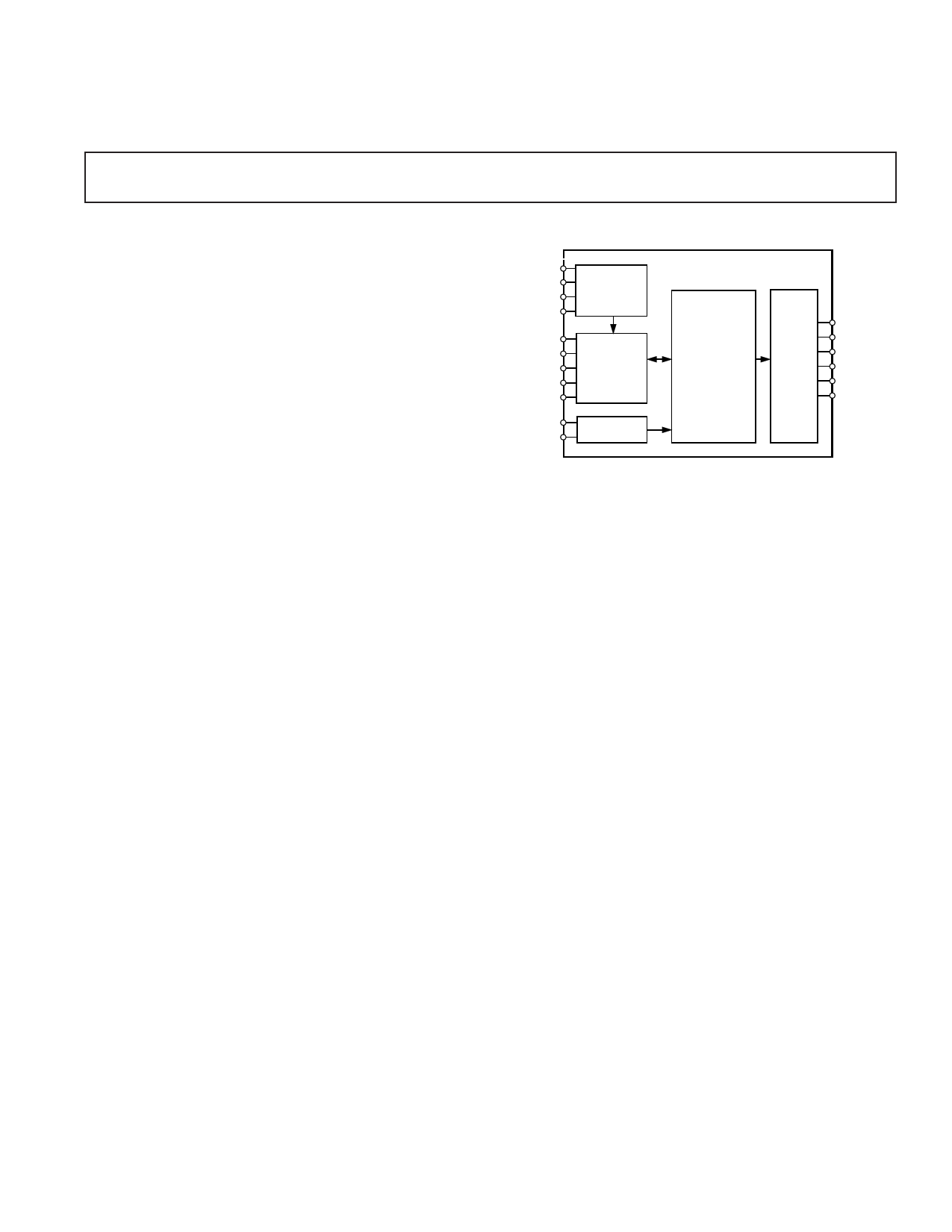
ADDC02803SC/ADDC02805SA
FUNCTIONAL BLOCK DIAGRAM
– SENSE
+ SENSE
ADJUST
STATUS
VAUX
INHIBIT
SYNC
ISHARE
TEMP
–VIN
+VIN
OUTPUT SIDE
CONTROL
CIRCUIT
INPUT SIDE
CONTROL
CIRCUIT
EMI FILTER
ADDC02803SC
ADDC02805SA
FIXED
FREQUENCY
DUAL
INTERLEAVED
POWER TRAIN
OUTPUT
FILTER
RETURN
RETURN
RETURN
+VOUT
+VOUT
+VOUT
GENERAL DESCRIPTION
The ADDC02803SC and ADDC02805SA hybrid dc/dc con-
verters with integral EMI filters offer the highest power density
of any dc/dc converter with their features and in their power
range available today. The converters with integral EMI filters
are fixed frequency, 1 MHz square wave switching dc/dc power
supplies. They are not variable frequency resonant converters.
In addition to many protection features, these converters have
system level features that allow them to be used as components
in larger systems as well as stand-alone power supplies. The
units are designed for high reliability and high performance
applications where saving space and/or weight are critical.
The ADDC02803SC and ADDC02805SA are available in
three screening grades; all grades use a hermetically sealed,
molybdenum based hybrid package. Three screening levels
are available, including military SMD.
PRODUCT HIGHLIGHTS
1. Up to 60 W/cubic inch power density with an integral EMI
filter designed to meet all applicable requirements in MIL-
STD-461D when installed in a typical system setup.
2. Light weight: 80 grams
3. Operational and survivable over a wide range of input condi-
tions: 16 V–50 V dc; survives low line, high line and positive
and negative transients. See section entitled: Input Voltage
Range.
4. High reliability; NAVMAT derated
5. Protection features include:
Output Overvoltage Protection
Output Short Circuit Current Protection
Thermal Monitor/Shutdown
Input Overvoltage Shutdown
Input Transient Protection
6. System level features include:
Current Sharing for Parallel Operation
Inhibit Control
Output Status Signal
Synchronization for Multiple Units
Input Referenced Auxiliary Voltage Supply
REV. A
Information furnished by Analog Devices is believed to be accurate and
reliable. However, no responsibility is assumed by Analog Devices for its
use, nor for any infringements of patents or other rights of third parties
which may result from its use. No license is granted by implication or
otherwise under any patent or patent rights of Analog Devices.
One Technology Way, P.O. Box 9106, Norwood, MA 02062-9106, U.S.A.
Tel: 781/329-4700 World Wide Web Site: http://www.analog.com
Fax: 781/326-8703
© Analog Devices, Inc., 1998
1 page 
100
90
1V
VO
ADDC02803SC/ADDC02805SA
50mV
100
90
50mV
VO
10
0%
10V
VINHIBIT
2ms
10
10A 0%
IO
50s
Figure 7. Output Voltage Transient During Turn-On with
Minimum Load Displaying Soft Start When Supply Is
Enabled (ADDC02805SA)
100
1V 90
VO
5V
10
0%
VINHIBIT
0.2ms
Figure 8. Output Voltage Transient During Turn-On with
Minimum Load Displaying Soft Start When Supply Is
Enabled (ADDC02803SC)
100mV 100
90
10
10A 0%
VO
IO
50s
Figure 9. Output Voltage Transient Response to
a 10 A to 20 A Step Change in Load with Zero Load
Capacitance (ADDC02805SA)
Figure 10. Output Voltage Transient Response to
a 10 A to 20 A Step Change in Load with Zero Load
Capacitance (ADDC02803SC)
0
–10
–20
–30
–40
–50
–60
–70
–80
–90
–100
10
100 1k
FREQUENCY – Hz
10k 50k
Figure 11. Audio Susceptibility (Magnitude of VOUT/VIN)
(ADDC02805SA)
0
–10
–20
–30
–40
–50
–60
–70
–80
–90
–100
10
100 1k 10k
FREQUENCY – Hz
50k
Figure 12. Audio Susceptibility (Magnitude of VOUT/VIN)
(ADDC02803SC)
REV. A
–5–
5 Page 
ADDC02803SC/ADDC02805SA
before it falls below 50 V. In both cases, the ADDC02803SC/
ADDC02805SA can be modified to operate to specification up
to the 50 V input voltage limit and to shut down and protect
itself during the time the input voltage exceeds 50 V. When the
input voltage falls below 50 V as the surge ends, the converter
will automatically initiate a soft start. In order to survive these
higher input voltage surges, the modified converter will no longer
have input transient protection, however, as described below.
Contact the factory for information on units surviving high
input voltage surges.
Input Voltage Transient Protection: The converter has a
transient voltage suppressor connected across its input leads to
protect the unit against high voltage pulses (both positive and
negative) of short duration. With the power supply connected
in the typical system setup shown in Figure 23, a transient
voltage pulse is created across the converter in the following
manner. A 20 µF capacitor is first charged to 400 V. It is then
directly connected across the converter’s end of the two meter
power lead cable through a 2 Ω on-state resistance MOSFET.
The duration of this connection is 10 µs. The pulse is repeated
every second for 30 minutes. This test is repeated with the
connection of the 20 µF capacitor reversed to create a negative
pulse on the supply leads. (If continuous reverse voltage
protection is required, a diode can be added externally in series
at the expense of lower efficiency for the power system.)
The converter responds to this input transient voltage test by
shutting down due to its input overvoltage protection feature.
Once the pulse is over, the converter initiates a soft-start, which
is completed before the next pulse. No degradation of converter
performance occurs.
THERMAL CHARACTERISTICS
Junction and Case Temperatures: It is important for the
user to know how hot the hottest semiconductor junctions
within the converter get, and to understand the relationship
between junction, case and ambient temperatures. The hottest
semiconductors in the 100 W product line of Analog Devices’
high density power supplies are the switching MOSFETs and
the output rectifiers. There is an area inside the main power
transformers that is hotter than these semiconductors, but it is
within NAVMAT guidelines and well below the Curie tempera-
ture of the ferrite. (The Curie temperature is the point at which
the ferrite begins to lose its magnetic properties.)
Since NAVMAT guidelines require that the maximum junction
temperature be 110°C, the power supply manufacturer must
specify the temperature rise above the case for the hottest semi-
conductors so the user can determine the case temperature
required to meet NAVMAT guidelines. The thermal charac-
teristics section of the specification table states the hottest junc-
tion temperature for maximum output power at a specified case
temperature. The unit can operate to case temperatures higher
than 90°C, but 90°C is the maximum temperature that permits
NAVMAT guidelines to be met.
Case and Ambient Temperatures: It is the user’s responsi-
bility to properly heat sink the power supply in order to maintain
the appropriate case temperature and, in turn, the maximum
junction temperature. Maintaining the appropriate case tem-
perature is a function of the ambient temperature and the me-
chanical heat removal system. The static relationship of these
variables is established by the following formula:
where:
TC = TA + ( P D × RθCA )
TC = case temperature measured at the center of the pack-
age bottom,
TA = ambient temperature of the air available for cooling,
PD = the power, in watts, dissipated in the power supply,
RθCA = the thermal resistance from the center of the package
to free air, or case to ambient.
The power dissipated in the power supply, PD, can be calcu-
lated from the efficiency, , given in the data sheets, and the
actual output power, PO, in the user’s application by the fol-
lowing formula:
PD
=
PO
1
η
– 1
For example, at 80 W of output power and 80% efficiency, the
power dissipated in the power supply is 20 W. If under these
conditions, the user wants to maintain NAVMAT deratings
(i.e., a case temperature of approximately 90°C) with an ambi-
ent temperature of 75°C, the required thermal resistance, case
to ambient, can be calculated as
90 = 75 + (20 × RθCA) or RθCA = 0.75°C/W
This thermal resistance, case to ambient, will determine what
kind of heat sink and whether convection cooling or forced air
cooling is required to meet the constraints of the system.
SYSTEM INSTABILITY CONSIDERATIONS
In a distributed power supply architecture, a power source
provides power to many “point-of-load” (POL) converters. At
low frequencies, the POL converters appear incrementally as
negative resistance loads. This negative resistance could cause
system instability problems.
Incremental Negative Resistance: A POL converter is de-
signed to hold its output voltage constant no matter how its
input voltage varies. Given a constant load current, the power
drawn from the input bus is therefore also a constant. If the
input voltage increases by some factor, the input current must
decrease by the same factor to keep the power level constant.
In incremental terms, a positive incremental change in the
input voltage results in a negative incremental change in the
input current. The POL converter therefore looks, incremen-
tally, like a negative resistor.
The value of this negative resistor at a particular operating
point, VIN, IIN, is:
RN
=
–VIN
I IN
Note that this resistance is a function of the operating point. At
full load and low input line, the resistance is its smallest, while
at light load and high input line, it is its largest.
REV. A
–11–
11 Page | ||
| Páginas | Total 18 Páginas | |
| PDF Descargar | [ Datasheet ADDC02803SCKV.PDF ] | |
Hoja de datos destacado
| Número de pieza | Descripción | Fabricantes |
| ADDC02803SCKV | 28 V/66 W/100 W DC/DC Converters with Integral EMI Filter | Analog Devices |
| Número de pieza | Descripción | Fabricantes |
| SLA6805M | High Voltage 3 phase Motor Driver IC. |
Sanken |
| SDC1742 | 12- and 14-Bit Hybrid Synchro / Resolver-to-Digital Converters. |
Analog Devices |
|
DataSheet.es es una pagina web que funciona como un repositorio de manuales o hoja de datos de muchos de los productos más populares, |
| DataSheet.es | 2020 | Privacy Policy | Contacto | Buscar |