|
|
|
PDF HS-81C55RH Data sheet ( Hoja de datos )
| Número de pieza | HS-81C55RH | |
| Descripción | Radiation Hardened 256 x 8 CMOS RAM | |
| Fabricantes | Intersil Corporation | |
| Logotipo | ||
Hay una vista previa y un enlace de descarga de HS-81C55RH (archivo pdf) en la parte inferior de esta página. Total 14 Páginas | ||
|
No Preview Available !
March 1996
HS-81C55RH,
HS-81C56RH
Radiation Hardened
256 x 8 CMOS RAM
Features
• Devices QML Qualified in Accordance with
MIL-PRF-38535
• Detailed Electrical and Screening Requirements are
Contained in SMD# 5962-95818 and Intersil’ QM Plan
• Radiation Hardened EPI-CMOS
- Parametrics Guaranteed 1 x 10⁵ RAD(Si)
- Transient Upset > 1 x 10⁸ RAD(Si)/s
- Latch-Up Free > 1 x 10¹² RAD(Si)/s
• Electrically Equivalent to Sandia SA 3001
• Pin Compatible with Intel 8155/56
• Bus Compatible with HS-80C85RH
• Single 5V Power Supply
• Low Standby Current 200µA Max
• Low Operating Current 2mA/MHz
• Completely Static Design
• Internal Address Latches
• Two Programmable 8-Bit I/O Ports
• One Programmable 6-Bit I/O Port
• Programmable 14-Bit Binary Counter/Timer
• Multiplexed Address and Data Bus
• Self Aligned Junction Isolated (SAJI) Process
• Military Temperature Range -55oC to +125oC
Description
The HS-81C55/56RH are radiation hardened RAM and I/O
chips fabricated using the Intersil radiation hardened Self-
Aligned Junction Isolated (SAJI) silicon gate technology.
Latch-up free operation is achieved by the use of epitaxial
starting material to eliminate the parasitic SCR effect seen in
conventional bulk CMOS devices.
The HS-81C55/56RH is intended for use with the
HS-80C85RH radiation hardened microprocessor system. The
RAM portion is designed as 2048 static cells organized as 256
x 8. A maximum post irradiation access time of 500ns allows
the HS-81C55/56RH to be used with the HS-80C85RH CPU
without any wait states. The HS-81C55RH requires an active
low chip enable while the HS-81C56RH requires an active high
chip enable. These chips are designed for operation utilizing a
single 5V power supply.
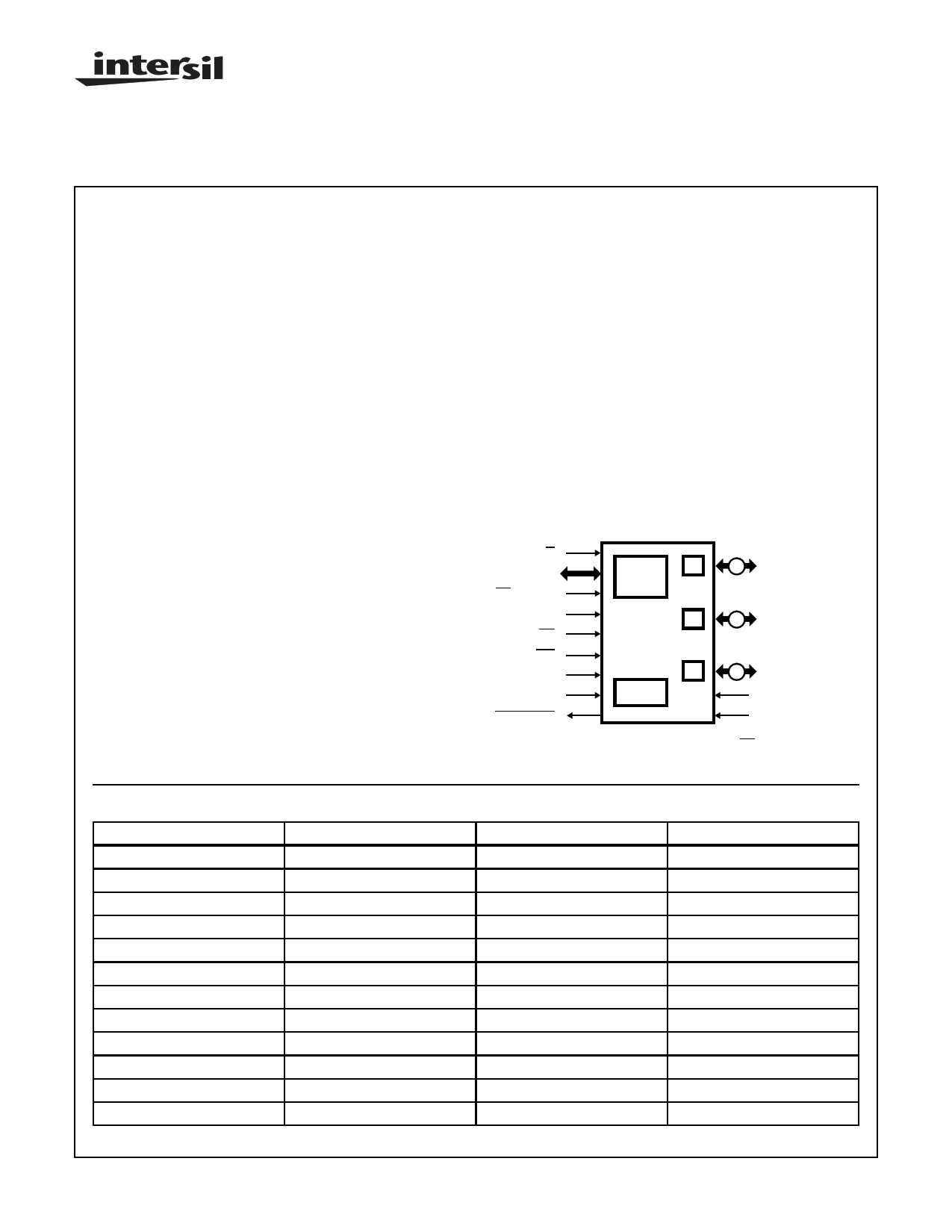
Functional Diagram
IO/M
AD0 - AD7
CE OR CE†
ALE
RD
WR
RESET
TIMER CLK
TIMER OUT
256 x 8
STATIC
RAM
PORT A
A 8 PA0 - PA7
PORT B
B 8 PB0 - PB7
TIMER
PORT C
C 8 PC0 - PC5
VDD (10V)
GND
†81C55RH = CE
81C56RH = CE
Ordering Information
PART NUMBER
5962R9XXXX01QRC
5962R9XXXX01VRC
5962R9XXXX01QXC
5962R9XXXX01VXC
5962R9XXXX02QRC
5962R9XXXX02VRC
5962R9XXXX02QXC
5962R9XXXX02VXC
HS1-81C55RH/Sample
HS9-81C55RH/Sample
HS1-81C56RH/Sample
HS9-81C56RH/Sample
TEMPERATURE RANGE
-55oC to +125oC
-55oC to +125oC
-55oC to +125oC
-55oC to +125oC
-55oC to +125oC
-55oC to +125oC
-55oC to +125oC
-55oC to +125oC
+25oC
+25oC
+25oC
+25oC
SCREENING LEVEL
MIL-PRF-38535 Level Q
MIL-PRF-38535 Level V
MIL-PRF-38535 Level Q
MIL-PRF-38535 Level V
MIL-PRF-38535 Level Q
MIL-PRF-38535 Level V
MIL-PRF-38535 Level Q
MIL-PRF-38535 Level V
Sample
Sample
Sample
Sample
PACKAGE
40 Lead SBDIP
40 Lead SBDIP
42 Lead Ceramic Flatpack
42 Lead Ceramic Flatpack
40 Lead SBDIP
40 Lead SBDIP
42 Lead Ceramic Flatpack
42 Lead Ceramic Flatpack
40 Lead SBDIP
42 Lead Ceramic Flatpack
40 Lead SBDIP
42 Lead Ceramic Flatpack
CAUTION: These devices are sensitive to electrostatic discharge; follow proper IC Handling Procedures.
http://www.intersil.com or 407-727-9207 | Copyright © Intersil Corporation 1999
1
Spec Number 518056
File Number 3039.1
1 page 
Specifications HS-81C55RH, HS-81C56RH
TABLE 2. AC ELECTRICAL PERFORMANCE CHARACTERISTICS (Continued)
PARAMETERS
GROUP A
SYMBOL CONDITIONS SUBGROUPS TEMPERATURE
LIMITS
MIN MAX UNITS
WRITE to Port Output
Port Input Setup Time
Port Input Hold Time
Strobe to Buffer Full
Strobe Width
READ to Buffer Empty
Strobe to INTR Off
READ to INTR Off
Port Setup Time to Strobe
Post Hold Time After Strobe
Strobe to Buffer Empty
WRITE to Buffer full
WRITE to INTR Off
TIMER-IN to TIMER OUT Low
TIMER-IN to TIMER-OUT High
Data Bus Enable from READ Control
TIMER-IN Low Time
TIMER-IN High Time
TWP
TPR
TRP
TSBF
TSS
TRBE
TSI
TRDI
TPSS
TPHS
TSBE
TWBF
TWI
TTL
TTH
TRDE
T1
T2
Notes 1, 4
Notes 1, 4
Notes 1, 4
Notes 1, 4
Notes 1, 4
Notes 1, 4
Notes 1, 4
Notes 1, 4
Notes 1, 4, 5
Notes 1, 4
Notes 1, 4
Notes 1, 4
Notes 1, 4
Notes 1, 4
Notes 1, 4
Notes 1, 4
Notes 1, 4, 6
Notes 1, 4
9, 10, 11
9, 10, 11
9, 10, 11
9, 10, 11
9, 10, 11
9, 10, 11
9, 10, 11
9, 10, 11
9, 10, 11
9, 10, 11
9, 10, 11
9, 10, 11
9, 10, 11
9, 10, 11
9, 10, 11
9, 10, 11
9, 10, 11
9, 10, 11
-55oC ≤ TA ≤ +125oC
-55oC ≤ TA ≤ +125oC
-55oC ≤ TA ≤ +125oC
-55oC ≤ TA ≤ +125oC
-55oC ≤ TA ≤ +125oC
-55oC ≤ TA ≤ +125oC
-55oC ≤ TA ≤ +125oC
-55oC ≤ TA ≤ +125oC
-55oC ≤ TA ≤ +125oC
-55oC ≤ TA ≤ +125oC
-55oC ≤ TA ≤ +125oC
-55oC ≤ TA ≤ +125oC
-55oC ≤ TA ≤ +125oC
-55oC ≤ TA ≤ +125oC
-55oC ≤ TA ≤ +125oC
-55oC ≤ TA ≤ +125oC
-55oC ≤ TA ≤ +125oC
-55oC ≤ TA ≤ +125oC
-
50
15
-
150
-
-
100
100
-
-
-
-
-
120
40
115
300
-
-
300
-
300
300
360
-
-
300
300
340
300
300
-
-
-
ns
ns
ns
ns
ns
ns
ns
ns
ns
ns
ns
ns
ns
ns
ns
ns
ns
ns
NOTES:
1. All devices guaranteed at worst case limits and over radiation.
2. Operating supply current (IDDOP) is proportional to operating frequency.
3. Output timings are measured with purely capacitive load.
4. For design purposes the limits are given as shown. For compatibility with the 80C85RH microprocessor, the AC parameters are tested
as maximums.
5. Parameter tested as part of the functional test. No read and record data available.
6. At low temperature, T1 is measured down to 10ns. If the reading is less than 10ns, the parameter will read 10ns.
7. Read and Record data available on failing data only.
TABLE 3. ELECTRICAL PERFORMANCE CHARACTERISTICS
LIMITS
PARAMETERS
Input Capacitance
I/O Capacitance
Output Capacitance
Data Bus Float After
READ
Recovery Time Between
Controls
SYMBOL
CIN
CI/O
COUT
TRDF
CONDITIONS
VDD = Open, f = 1MHz, All measurements
referenced to device ground
VDD = Open, f = 1MHz, All measurements
referenced to device ground
VDD = Open, f = 1MHz, All measurements
referenced to device ground
VDD = 4.75V
TRV
VDD = 4.75V
TEMPERATURE MIN MAX UNITS
TA = +25oC
- 10 pF
TA = +25oC
- 12 pF
TA = +25oC
- 10 pF
-55oC, +25oC,
+125oC
-55oC, +25oC,
+125oC
10 100
- 220
ns
ns
NOTE: The parameters listed in Table 3 are controlled via design or process parameters and are not directly tested. These parameters are
characterized upon initial design release and upon design changes which would affect these characteristics.
Spec Number 518056
5
5 Page 
HS-81C55RH, HS-81C56RH
Input/Output Section
The I/O section of the HS-81C55RH and HS-81C56RH
consists of five registers: (See Figure 5)
• Command/Status Register (C/S) - Both register are
assigned the address XXXXX000. The C/S address
serves the dual prupose.
When the C/S registers are selected during WRITE
operation, a command is written into the command
register. The contents of this register are not accessible
through the pins.
When the C/S (XXXXX000) is selected during a READ
operation, the status information of the I/O ports and the
timer becomes available on the AD0 - AD7 lines.
• PA Register - This register can be programmed to be
either input or output ports depending on the status of the
contents of the C/S Register. also depending on the
command, this port can operate in either the basic mode
or the strobed mode (See timing diagram). the I/O pins
assigned in relation to this register are PA0 - PA7. The
address of this register is XXXXX001.
• PB Register - This register functions the same as PA
Register. the I/O pins assigned are PB0 - PB7. The
address of this register is XXXXX010
• PC Register - This register has the address XXXXX011
and contains only 6 bits. The 6 bits can be programmed to
be either input ports, output ports or as control signals for
PA and PB by properly programming the AD2 and AD3
bits of the C/S register.
When PC0 - PC5 is used as a control port, 3 bits are
assigned for Port A and 3 for Port B. The first bit is an
Interrupt that the HS-81C55RH and HS-81C56RH sends
out. The second is an output signal indicating whether the
buffer is full or empty, and the third is an input pin to
accept a strobe for the strobed input mode. (See Table 1).
When the ‘C’ port is programmed to either ALT3 or ALT4, the
control signals for PA and Pb are initialized as follows: :
CONTROL
BF
INTR
STB
INPUT MODE
Low
Low
Input Control
OUTPUT MODE
Low
High
Input Control
I/O ADDRESS†
A7 A6 A5 A4 A3 A2 A1 A0
SELECTION
X X X X X 0 0 0 Interval Command/
Status Register
X X X X X 0 0 1 General Purpose I/O
Port A
X X X X X 0 1 0 General Purpose I/O
Port B
X X X X X 0 1 1 General Purpose I/O or
Control Port C
X X X X X 1 0 0 Low-Order 8 Bits of
Timer Count
X X X X X 1 0 1 High 6 Bits of Timer
Count and 2 Bits of Timer
Mode
† I/O Address must be qualified by CE = 1(81C56RH) or CE =
0(81C55RH) and IO/M = 1 in order to select the appropriate register.
X = Don’t Care
FIGURE 5. I/O PORT AND TIMER ADDRESSING SCHEME
Figure 6 shows how I/O Ports A and B are structured within
the HS-81C55RH and HS-81C56RH.
Note in the diagram that when the I/O ports are programmed
to be output ports, the contents of the output ports can still
be read by a READ operation when appropriately
addressed.
HS-81C55RH AND HS-81C56RH
ONE BIT OF PORT A OR PORT B
OUTPUT
D LATCH Q
CLK CLR
(1) OUTPUT MODE
(2) SIMPLE INPUT
(3) STROBED INPUT
MULTIPLEXER
CONTROL
(4) = 1 FOR OUTPUT MODE
= 0 FOR INPUT MODE
PA/PB
PIN
WRITE
PORT
MUX (1)
(2)
MODE (4)
READ
PORT
(3)
LATCH
QD
CLK
NOTES:
1. READ Port = (IO/M = 1)(RD = 0)(CE Active)
(Port Address Selected)
2. WRITE Port = (IO/M = 1)(wr = 0)(CE Active)
(Port Address Selected)
STB
FIGURE 6. HS-81C55RH AND HS-81C56RH PORT FUNCTION
Spec Number 518056
11
11 Page | ||
| Páginas | Total 14 Páginas | |
| PDF Descargar | [ Datasheet HS-81C55RH.PDF ] | |
Hoja de datos destacado
| Número de pieza | Descripción | Fabricantes |
| HS-81C55RH | Radiation Hardened 256 x 8 CMOS RAM | Intersil Corporation |
| Número de pieza | Descripción | Fabricantes |
| SLA6805M | High Voltage 3 phase Motor Driver IC. |
Sanken |
| SDC1742 | 12- and 14-Bit Hybrid Synchro / Resolver-to-Digital Converters. |
Analog Devices |
|
DataSheet.es es una pagina web que funciona como un repositorio de manuales o hoja de datos de muchos de los productos más populares, |
| DataSheet.es | 2020 | Privacy Policy | Contacto | Buscar |