|
|
|
PDF LTC1771E Data sheet ( Hoja de datos )
| Número de pieza | LTC1771E | |
| Descripción | Low Quiescent Current High Efficiency Step-Down DC/DC Controller | |
| Fabricantes | Linear Technology | |
| Logotipo | ||
Hay una vista previa y un enlace de descarga de LTC1771E (archivo pdf) en la parte inferior de esta página. Total 16 Páginas | ||
|
No Preview Available !
FEATURES
s Very Low Standby Current: 10µA
s Available in Space-Saving 8-Lead MSOP Package
s High Output Currents
s Wide VIN Range: 2.8V to 20V Operation
s VOUT Range: 1.23V to 18V
s High Efficiency: Over 93% Possible
s ±2% Output Accuracy
s Very Low Dropout Operation: 100% Duty Cycle
s Current Mode Operation for Excellent Line and
Load Transient Response
s Defeatable Burst ModeTM Operation
s Short-Circuit Protected
s Optional Programmable Soft-Start
s Micropower Shutdown: IQ = 2µA
U
APPLICATIO S
s Cellular Telephones and Wireless Modems
s 1- to 4-Cell Lithium-Ion-Powered Applications
s Portable Instruments
s Battery-Powered Equipment
s Battery Chargers
s Scanners
Final Electrical Specifications
LTC1771
Low Quiescent Current
High Efficiency Step-Down
DC/DC Controller
DESCRIPTIO
February 2000
The LTC®1771 is a high efficiency current mode step-
down DC/DC controller that draws as little as 10µA DC
supply current to regulate the output at no load while
maintaining high efficiency for loads up to several amps.
The LTC1771 drives an external P-channel power MOSFET
using a current mode, constant off-time architecture. An
external sense resistor is used to program the operating
current level. Current mode control provides short-circuit
protection, excellent transient response and controlled
start-up behavior. Burst Mode operation enables the
LTC1771 to maintain high efficiency down to extremely
low currents. Shutdown mode further reduces the supply
current to a mere 2µA. For low noise applications, Burst
Mode operation can be easily disabled with the MODE pin.
Wide input supply range of 2.8V to 18V (20V maximum)
and 100% duty cycle operation for low dropout make the
LTC1771 ideal for a wide variety of battery-powered appli-
cations where maximizing battery life is important.
The LTC1771’s availability in both 8-lead MSOP and SO
packages provides for a minimum area solution.
, LTC and LT are registered trademarks of Linear Technology Corporation.
Burst Mode is a trademark of Linear Technology Corporation.
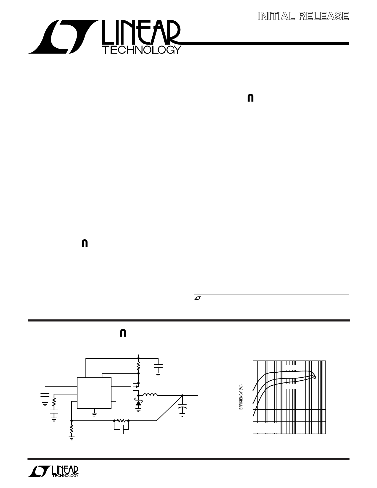
TYPICAL APPLICATIO
CSS
0.01µF
VIN
4.5V TO 18V
RSENSE
0.05Ω
10µF
25V
CER
RC
10k
CC
22OpF
VIN SENSE
RUN/SS PGATE
ITH LTC1771
VFB MODE
GND
M1
Si6447DQ
VIN
R2
1.64M
1%
R1
1M
1%
5pF
L1
15µH
UPS5817
VOUT
3.3V
+ COUT 2A
150µF
6.3V
1771 F01
Figure 1. High Efficiency Step-Down Converter
LTC1771 Efficiency
100
VIN = 5V
90 VIN = 10V
80 VIN = 15V
70
60
50
VOUT = 3.3V
40 RSENSE = 0.05Ω
0.1 1
10
100 1000
LOAD CURRENT (mA)
10000
1771 F01b
Information furnished by Linear Technology Corporation is believed to be accurate and reliable.
However, no responsibility is assumed for its use. Linear Technology Corporation makes no represen-
tation that the interconnection of its circuits as described herein will not infringe on existing patent rights.
1
1 page 
U
OPERATIO (Refer to Functional Block Diagram)
Main Control Loop
The LTC1771 uses a constant off-time, current mode
step-down architecture. During normal operation, the
P-channel MOSFET is turned on at the beginning of each
cycle and turned off when the current comparator C
triggers the 1-shot timer. The external MOSFET switch
stays off for the 3.5µs 1-shot duration and then turns back
on again to begin a new cycle. The peak inductor current
at which C triggers the 1-shot is controlled by the voltage
on Pin 3 (ITH), the output of the error amplifier EA. An
external resistive divider connected between VOUT and
ground allows EA to receive an output feedback voltage
VFB. When the load current increases, it causes a slight
decrease in VFB relative to the 1.23V reference, which in
turn causes the ITH voltage to increase until the average
inductor current matches the new load current.
The main control loop is shut down by pulling Pin 1
(RUN/SS) low. Releasing RUN/SS allows an internal 1µA
current source to charge soft-start capacitor CSS. When
CSS reaches 1V, the main control loop is enabled with the
ITH voltage clamped at approximately 40% of its maxi-
mum value. As CSS continues to charge, ITH is gradually
released allowing normal operation to resume.
Burst Mode Operation
The LTC1771 provides outstanding low current efficiency
and ultralow no-load supply current by using Burst Mode
operation when the MODE pin is pulled above 2V. During
Burst Mode operation, short burst cycles of normal switch-
ing are followed by a longer idle period with the switch off
and the load current is supplied by the output capacitor.
During this idle period, only the minimum required cir-
cuitry—1.23V reference and error amp—are left on, and
the supply current is reduced to 9µA. At no load, the output
capacitor is still discharged very slowly by leakage current
in the Schottky diode and feedback resistor current result-
ing in very low frequency burst cycles that add a few more
microamps to the supply current.
LTC1771
Burst Mode operation is provided by clamping the mini-
mum ITH voltage at 1V which represents about 25% of
maximum load current. If the load falls below this level, i.e.
the ITH voltage tries to fall below 1V, the burst comparator
B switches state signaling the LTC1771 to enter sleep
mode. During this time, EA is reduced to 10% of its normal
operating current and the external compensation capaci-
tor is disconnected and clamped to 1V so that the EA can
drive its output with the lower available current. As the load
discharges the output capacitor, the internal ITH voltage
increases. When it exceeds 1V the burst comparator exits
sleep mode, reconnects the external compensation com-
ponents to the error amplifier output, and returns EA to full
power along with the other necessary circuitry. This
scheme (patent pending) allows the EA to be reduced to
such a low operating current during sleep mode without
adding unacceptable delay to wake up the LTC1771 due to
the compensation capacitor on ITH required for stability in
normal operation.
Burst Mode operation can be disabled by pulling the
MODE pin to ground. In this mode of operation, the burst
comparator B is disabled and the ITH voltage allowed to go
all the way to 0V. The load can now be reduced to about 1%
of maximum load before the loop skips cycles to maintain
regulation. This mode provides a low noise output spec-
trum, useful for reducing both audio and RF interference,
at the expense of reduced efficiency at light loads.
Off-Time
The off-time duration is 3.5µs when the feedback voltage
is close to the reference voltage; however, as the feedback
voltage drops, the off-time lengthens and reaches a maxi-
mum value of about 70µs when VFB is zero. This ensures
that the inductor current has enough time to decay when
the reverse voltage across the inductor is low such as
during short circuit, thus protecting the MOSFET and
inductor.
5
5 Page 
LTC1771
APPLICATIO S I FOR ATIO
Design Example
As a design example, assume VIN = 10V (nominal), VIN =
15V(MAX), VOUT = 3.3V, and IMAX = 2A. With this informa-
tion, we can easily calculate all the important components.
RSENSE = 100mV/2A = 0.05Ω
To optimize low current efficiency, MODE pin is tied to VIN
to enable Burst Mode operation, thus the minimum induc-
tance necessary is:
LMIN = 70µH(3.3V + 0.5)(0.05Ω) = 13.3µH
15µH is chosen for the application.
∆IL
=
3.5µs
3.3V + 0.5V
15µH
=
0.89A
For the feedback resistors, choose R1 = 1M to minimize
supply current. R2 can then be calculated to be:
R2 = (VOUT/1.23 – 1) • R1 = 1.68M
Assume that the MOSFET dissipation is to be limited to
PP = 0.25W.
If TA = 70°C and the thermal resistance of the MOSFET is
83°C/W, then the junction temperatures will be 91°C and
δP = 0.33. The required RDS(ON) for the MOSFET can now
be calculated:
( ) ( )P -Channel
RDS(ON)
=
0.25W
3.3V + 0.5V
10V + 0.5V
2A
2
1.33
= 0.130Ω
Since the gate of the MOSFET will see the full input voltage,
a MOSFET must be selected whose VGS(MAX) > 15V. A
P-channel MOSFET that meets both the VGS(MAX) and
RDS(ON) requirement is the Si6447DQ.
The most stringent requirement for the Schottky diode
occurs when VOUT = 0V (i.e., short circuit) at maximum
VIN. In this case the worst-case dissipation rises to:
( )PD
= ISC(AVG)
VD
VIN
VIN + VD
With a 0.05Ω sense resistor ISC(AVG) = 2A will result,
increasing the 0.5V Schottky diode dissipation to 1W.
CIN is chosen for a RMS current rating of at least 1A at
temperature. COUT is chosen with an ESR of 0.05Ω for low
output ripple. The output voltage ripple due to ESR is
approximately:
VORIPPLE ≈ (RESR)(∆IL) = 0.05Ω (0.89AP-P) = 45mVP-P
CSS
1
RUN/SS
CITH RITH
2
ITH
8
MODE
MODE
7
SENSE
R1
3 LTC1771
6
VFB VIN
4
GND
5
PGATE
+
CIN D1
Q1
R2 CFF 0.1µF
+ COUT
BOLD LINES INDICATE HIGH CURRENT PATHS
Figure 3. LTC1771 Layout Diagram
L
VOUT
1771 F03
11
11 Page | ||
| Páginas | Total 16 Páginas | |
| PDF Descargar | [ Datasheet LTC1771E.PDF ] | |
Hoja de datos destacado
| Número de pieza | Descripción | Fabricantes |
| LTC1771 | High Efficiency Step-Down DC/DC Controller | Linear Technology |
| LTC1771E | Low Quiescent Current High Efficiency Step-Down DC/DC Controller | Linear Technology |
| LTC1771EMS8 | Low Quiescent Current High Efficiency Step-Down DC/DC Controller | Linear Technology |
| LTC1771ES8 | Low Quiescent Current High Efficiency Step-Down DC/DC Controller | Linear Technology |
| Número de pieza | Descripción | Fabricantes |
| SLA6805M | High Voltage 3 phase Motor Driver IC. |
Sanken |
| SDC1742 | 12- and 14-Bit Hybrid Synchro / Resolver-to-Digital Converters. |
Analog Devices |
|
DataSheet.es es una pagina web que funciona como un repositorio de manuales o hoja de datos de muchos de los productos más populares, |
| DataSheet.es | 2020 | Privacy Policy | Contacto | Buscar |