|
|
|
PDF CXA1386P Data sheet ( Hoja de datos )
| Número de pieza | CXA1386P | |
| Descripción | 8-bit 75MSPS Flash A/D Converter | |
| Fabricantes | Sony Corporation | |
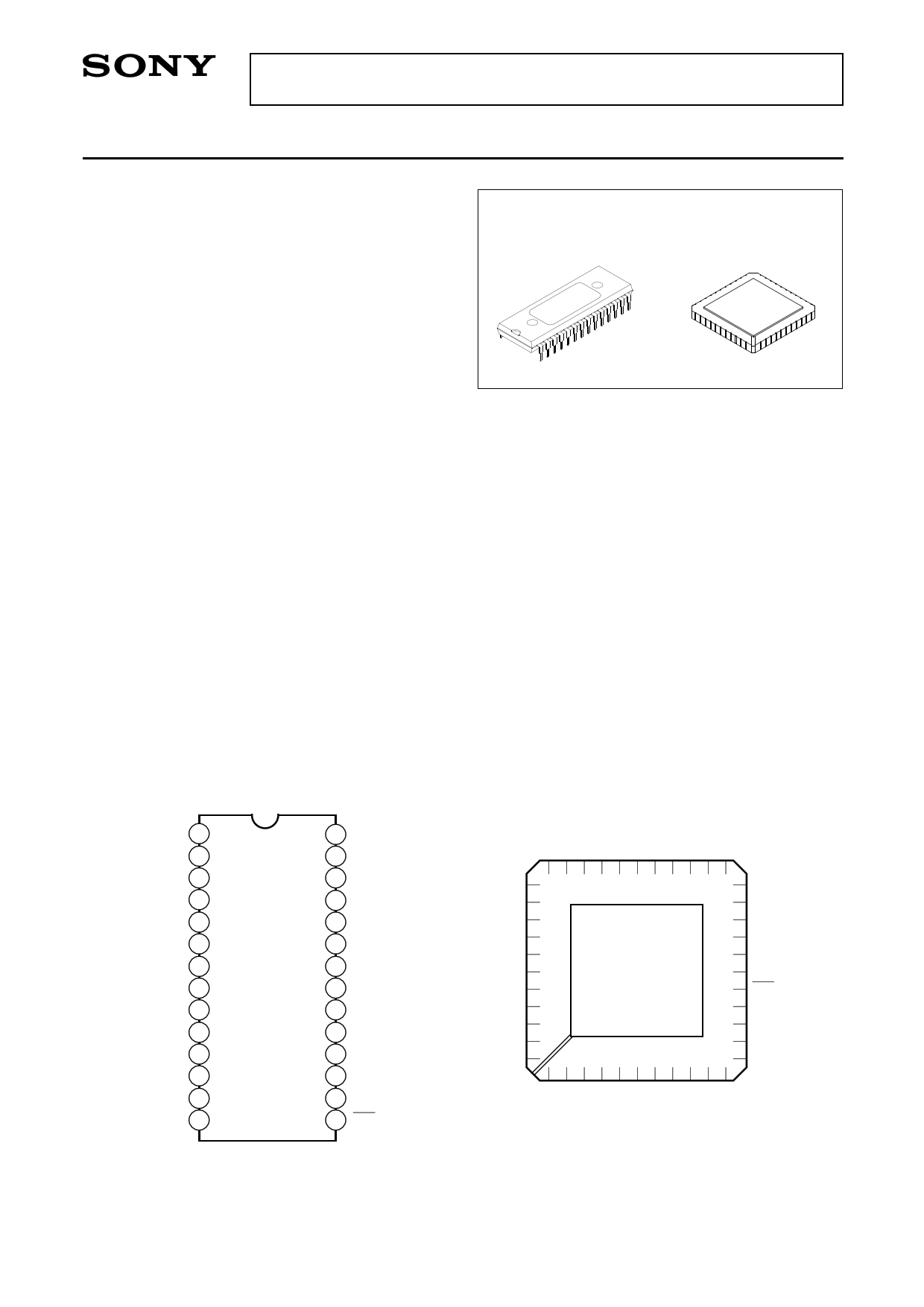
| Logotipo | ||
Hay una vista previa y un enlace de descarga de CXA1386P (archivo pdf) en la parte inferior de esta página. Total 21 Páginas | ||
|
No Preview Available !
CXA1386P/K
8-bit 75MSPS Flash A/D Converter
Description
The CXA1386P/K are 8-bit high-speed flash A/D
converter ICs capable of digitizing analog signals at
the maximum rate of 75MSPS. The digital I/O levels
of these A/D converters are compatible with the
ECL 100K/10KH/10K.
The CXA1386P/K is pin-compatible with the
earlier models CXA1056P/K, CXA1016P/K,
respectively. They can be replaced by the
CXA1386P/K without any design changes, in most
cases. Compared with the earlier models, these
new models have been greatly improved in
performance, by incorporating advanced process,
new circuit design and carefully considered layout.
Features
• Differential linearity error: ±1/2LSB or less
• Integral linearity error: ±1/2LSB or less
• High-speed operation with maximum conversion
rate of 75MSPS (Min.)
• Wide analog input bandwidth: 150MHz (Min. for
full-scale input)
• Low Power consumption: 580mW (Typ.)
• Single power supply: –5.2V
• Low input capacitance: 17pF (Typ.)
• Built-in integral linearity conpensation circuit
• Low error rate
• Operable at 50% clock duty cycle
• Good temperature characteristics
• Capable of driving 50Ω loads
Pin Configuration
Pins with name are NC pins (not connected).
LINV 1
DVEE 2
DGND 3
(LSB) D0 4
D1 5
D2 6
D3 7
D4 8
D5 9
D6 10
(MSB) D7 11
DGND 12
DVEE 13
MINV 14
CXA1386P
28 AVEE
27 VRT
26 AVEE
25 AGND
24 VIN
23 AGND
22 VRM
21 AGND
20 VIN
19 AGND
18 AVEE
17 VRB
16 CLK
15 CLK
CXA1386P
28 pin DIP (Plastic)
CXA1386K
44 pin LCC (Ceramic)
Structure
Bipolar silicon monolithic IC
Applications
• Digital oscilloscopes
• HDTV (high-definition TVs)
• Other apparatus requiring high-speed A/D
conversion
39
AVEE 40 38 37 36 35 34 33 32 31 30 29 28 AVEE
AVEE 41
27 AVEE
VRT 42
26 VRB
43 25
AVEE 44
24
1
CXA1386K
23 CLK
2 22 CLK
LINV 3
21 MINV
DVEE 4
20 DVEE
DGND1 5
19 DGND1
DGND2 6
18
8 9 10 11 12 13 14 15 16 17
7
Sony reserves the right to change products and specifications without prior notice. This information does not convey any license by
any implication or otherwise under any patents or other right. Application circuits shown, if any, are typical examples illustrating the
operation of the devices. Sony cannot assume responsibility for any problems arising out of the use of these circuits.
–1–
E90114C54-ST
1 page 
CXA1386P/K
Pin No
Symbol
LCC DIP
Standard
I/O voltage
level
4, 20 2, 13 DVEE — –5.2V
8 4 D0
9 5 D1
10 6 D2
11 7 D3
O ECL
12 8 D4
13 9 D5
14 10 D6
15 11 D7
Equivalent circuit
Description
Digital VEE
Internally connected
with AVEE
(resistance: 4 to 6Ω)
Ceramic chip
capacitors of at least
0.1µF should be used
to connect to DGND
and be placed near the
pins.
DGND (DGND2) LSB of data outputs.
External pull-down
resistor is required.
Di
Data outputs.
External pull-down
resistors are required.
MSB of data outputs.
External pull-down
DVEE
resistor is required.
DGND (DGND1)
3 1 LINV I ECL
LINV
or
MINV
r
r
r
21 14 MINV I ECL
DVEE
r
Input pin for D0 (LSB)
to D6 output polarity
inversion (see output
code table).
With open connection,
kept at "L" level.
–1.3V
Input pin for D7 (MSB)
output polarity
inversion (see output
code table).
With open connection,
kept at "L" level.
–5–
5 Page 
CXA1386P/K
8bit 75MSPS ADC and DAC Evaluation Board
It is necessary to equip "the CXA1396D/P EVALUATION BOARD WITH DAC" with "A1396D – A1386P
ADAPTER" in order to evaluate CXA1386P.
In addition to indispensable features such as the reference voltage generator, this tool equips two sets of
analog inputs (the direct input and the buffer amplifier input), the input voltage offset generator, the clock
decimator, the output data latches, the 10-bit high-speed DAC, and the 20-pin cable connector for digital
outputs. This evaluation board provides full performance of the CXA1386P and it is designed to facilitate
evaluation.
Features
Resolution: 8bits
Maximum conversion rate: 75MSPS
Supply voltage: +5.0V, –5.2V, –2.0V
Two analog inputs (Direct input, buffer amplifier input)
Clock level converter: Sine wave to ECL level signal
Reference voltage adjustment circuit for the A/D converter
Built-in clock frequency decimation circuit: (1/1 to 1/16)
Fig. 1. Block Diagram
–5.2V (A)
VR2 VRB
(2k) –2V
–5.2V (A)
VR1 Vin
(2k) OFFSET
AMP.IN
51
240
HL
VR3
(1k)
1k
X (–2)
51
SW1
SW2
LINV MINV
VRB
J1
A VRM
8
CXA1386P
B
C Vin
CLK
D
DIGITAL OUT
(CONNECTOR)
DATA
8
BUFFER
LATCH
(D7 to D0)
8
CLK
(D7 to D0) 8
2 (CLK.CLK)
DIR.IN
CLK
0.1µ
+5V –5.2V (A) AGND
DECIMATOR
SW3
1/1 to 1/16
D/A
CONVERTER
CLK
D/A OUT
–5.2V (D) DGND –2V (D)
– 11 –
11 Page | ||
| Páginas | Total 21 Páginas | |
| PDF Descargar | [ Datasheet CXA1386P.PDF ] | |
Hoja de datos destacado
| Número de pieza | Descripción | Fabricantes |
| CXA1386K | 8-bit 75MSPS Flash A/D Converter | Sony Corporation |
| CXA1386P | 8-bit 75MSPS Flash A/D Converter | Sony Corporation |
| Número de pieza | Descripción | Fabricantes |
| SLA6805M | High Voltage 3 phase Motor Driver IC. |
Sanken |
| SDC1742 | 12- and 14-Bit Hybrid Synchro / Resolver-to-Digital Converters. |
Analog Devices |
|
DataSheet.es es una pagina web que funciona como un repositorio de manuales o hoja de datos de muchos de los productos más populares, |
| DataSheet.es | 2020 | Privacy Policy | Contacto | Buscar |