|
|
|
PDF CXA3086 Data sheet ( Hoja de datos )
| Número de pieza | CXA3086 | |
| Descripción | 6-bit 140MSPS Flash A/D Converter | |
| Fabricantes | Sony Corporation | |
| Logotipo | ||
Hay una vista previa y un enlace de descarga de CXA3086 (archivo pdf) en la parte inferior de esta página. Total 30 Páginas | ||
|
No Preview Available !
CXA3086Q
6-bit 140MSPS Flash A/D Converter
Description
The CXA3086Q is an 6-bit high-speed flash A/D
converter capable of digitizing analog signals at the
maximum rate of 140MSPS. ECL, PECL or TTL can
be selected as the digital input level in accordance
with the application. The TTL digital output level
allows 1: 2 demultiplexed output.
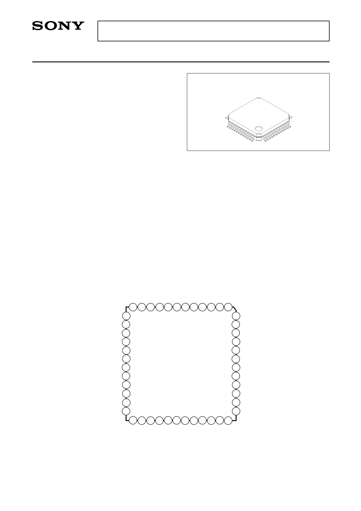
48 pin QFP (Plastic)
Features
• Differential linearity error: ±0.2LSB or less
• Integral linearity error: ±0.2LSB or less
• High-speed operation with a maximum conversion
rate of 140MSPS
Structure
Bipolar silicon monolithic IC
• Low input capacitance: 7pF
• Wide analog input bandwidth: 200MHz
• Low power consumption: 358mW
• Low error rate
• Excellent temperature characteristics
• 1: 2 demultiplexed output
Applications
• Magnetic recording (PRML)
• Communications (QPSK, QAM)
• LCDs
• Digital oscilloscopes
• 1/2 frequency divided clock output
(with reset function)
• Compatible with ECL, PECL and TTL digital input levels
• Single +5V power supply operation available
• Surface mounting package
Pin Configuration (Top View)
12 11 10 9 8 7 6 5 4 3 2 1
DVEE3 13
48 DVCC2
AGND 14
47 DVCC1
VRBS 15
46 DGND1
VRB 16
45 N.C.
AVCC 17
44 PS
N.C. 18
43 CLKOUT
VIN 19
42 INV
AVCC 20
41 SELECT
VRT 21
40 N.C.
VRTS 22
39 DGND1
AGND 23
38 DVCC1
DGND3 24
37 DVCC2
25 26 27 28 29 30 31 32 33 34 35 36
Sony reserves the right to change products and specifications without prior notice. This information does not convey any license by
any implication or otherwise under any patents or other right. Application circuits shown, if any, are typical examples illustrating the
operation of the devices. Sony cannot assume responsibility for any problems arising out of the use of these circuits.
–1–
E95619C77
1 page 
CXA3086Q
Pin
No.
Symbol
I/O
Standard
voltage level
27 CLK/T
I
Equivalent circuit
DVCC1
r/2
TTL
10 RESETN/T I
10 27
DGND1
DVEE3
1.5V
r
42 INV
I
DVCC1
44 PS
TTL
42 44
I
DGND1
DVEE3
DVCC1
Description
Clock input.
Reset input.
When left open, this input goes to
high level. When the input is set to
low level, the built-in CLK frequency
divider circuit can be reset.
Data output polarity inversion input.
When left open, this input goes to
high level.
(See Table 1. I/O Correspondence
Table.)
Power saving input.
When the input is set to low level,
the power saving mode is set.
In this time the all TTL outputs go
into the high-impedance state.
Normally, set to high level or left
open.
41 SELECT
Vcc
or
GND
22 VRTS
O
+4.0V
(typ.)
21 VRT
I VRTS
+r1 x Iref
16 VRB
I
VRBS
–r2 x Iref
15 VRBS
O
+2.0V
(typ.)
41
DGND1
DVEE3
Data output mode selection.
(See Table 2. Operating Mode
Table.)
22
r1
21
r
r
r
r
Comparator 1
Comparator 2
r2
16
15
r
r
r
r
Comparator 62
Comparator 63
Reference voltage sense.
By-pass to AGND with a 0.1µF chip
capacitor.
Top reference voltage.
By-pass to AGND with a 1µF tantal
capacitor and a 0.1µF chip
capacitor.
Bottom reference voltage.
By-pass to AGND with a 1µF tantal
capacitor and a 0.1µF chip
capacitor.
Reference voltage sense.
By-pass to AGND with a 0.1µF chip
capacitor.
–5–
5 Page 
When the RESET signal is not used.
CLK
CLK
CXA3086Q
CLK A A
RESETN
CLKOUT
6bit
DATA
CXA3086Q
CLK B B
RESETN
CLKOUT
6bit
DATA
When the RESET signal is used.
CLK
RESET signal
CXA3086Q
CLK A
RESETN
CLK
RESET signal
CLKOUT
6bit
DATA
(Reset period)
CXA3086Q
CLK B
RESETN
CLKOUT
6bit
DATA
(Reset period)
CXA3086Q
2. Straight mode (See Application Circuits (4), (5) and (6).)
Set the SELECT pin to GND for this mode. In this mode, data output can be obtained in accordance with the
clock frequency applied to the A/D converter for applications which use the clock applied to the A/D converter
as the system clock.
The A/D converter can operate at Fc (min.) = 100MSPS in this mode.
Digital input level and supply voltage settings
The logic input level for the CXA3086Q supports ECL, PECL and TTL levels.
The power supplies (DVEE3, DGND3) for the logic input block must be set to match the logic input (CLK and
RESET signals) level.
Digital input level
ECL
PECL
TTL
DVEE3
–5V
0V
0V
DGND3
0V
+5V
+5V
Supply voltage Application circuits
±5V (1) (4)
+5V (2) (5)
+5V (3) (6)
Table 3. Logic Input Level and Power Supply Settings
– 11 –
11 Page | ||
| Páginas | Total 30 Páginas | |
| PDF Descargar | [ Datasheet CXA3086.PDF ] | |
Hoja de datos destacado
| Número de pieza | Descripción | Fabricantes |
| CXA3085AN | All Band TV Tuner IC with On-chip PLL | Sony Corporation |
| CXA3086 | 6-bit 140MSPS Flash A/D Converter | Sony Corporation |
| CXA3086Q | 6-bit 140MSPS Flash A/D Converter | Sony Corporation |
| Número de pieza | Descripción | Fabricantes |
| SLA6805M | High Voltage 3 phase Motor Driver IC. |
Sanken |
| SDC1742 | 12- and 14-Bit Hybrid Synchro / Resolver-to-Digital Converters. |
Analog Devices |
|
DataSheet.es es una pagina web que funciona como un repositorio de manuales o hoja de datos de muchos de los productos más populares, |
| DataSheet.es | 2020 | Privacy Policy | Contacto | Buscar |