|
|
|
PDF FM24C02U Data sheet ( Hoja de datos )
| Número de pieza | FM24C02U | |
| Descripción | 2K-Bit Standard 2-Wire Bus Interface Serial EEPROM | |
| Fabricantes | Fairchild Semiconductor | |
| Logotipo | ||
Hay una vista previa y un enlace de descarga de FM24C02U (archivo pdf) en la parte inferior de esta página. Total 14 Páginas | ||
|
No Preview Available !
August 2000
FM24C02U/03U – 2K-Bit Standard 2-Wire Bus
Interface Serial EEPROM
General Description
The FM24C02U/03U devices are 2048 bits of CMOS non-volatile
electrically erasable memory. These devices conform to all speci-
fications in the Standard IIC 2-wire protocol. They are designed to
minimize device pin count and simplify PC board layout require-
ments.
The upper half (upper 1Kbit) of the memory of the FM24C03U can
be write protected by connecting the WP pin to VCC. This section of
memory then becomes unalterable unless WP is switched to VSS.
This communications protocol uses CLOCK (SCL) and DATA
I/O (SDA) lines to synchronously clock data between the master
(for example a microprocessor) and the slave EEPROM device(s).
The Standard IIC protocol allows for a maximum of 16K of
EEPROM memory which is supported by the Fairchild family in
2K, 4K, 8K, and 16K devices, allowing the user to configure the
memory as the application requires with any combination of
EEPROMs. In order to implement higher EEPROM memory
densities on the IIC bus, the Extended IIC protocol must be used.
(Refer to the FM24C32 or FM24C65 datasheets for more informa-
tion.)
Fairchild EEPROMs are designed and tested for applications requir-
ing high endurance, high reliability and low power consumption.
Features
I Extended operating voltage 2.7V – 5.5V
I 400 KHz clock frequency (F) at 2.7V - 5.5V
I 200µA active current typical
10µA standby current typical
1µA standby current typical (L)
0.1µA standby current typical (LZ)
I IIC compatible interface
– Provides bi-directional data transfer protocol
I Sixteen byte page write mode
– Minimizes total write time per byte
I Self timed write cycle
Typical write cycle time of 6ms
I Hardware Write Protect for upper half (FM24C03U only)
I Endurance: 1,000,000 data changes
I Data retention greater than 40 years
I Packages available: 8-pin DIP, 8-pin SO, and 8-pin TSSOP
I Available in three temperature ranges
- Commercial: 0° to +70°C
- Extended (E): -40° to +85C
- Automotive (V): -40° to +125°C
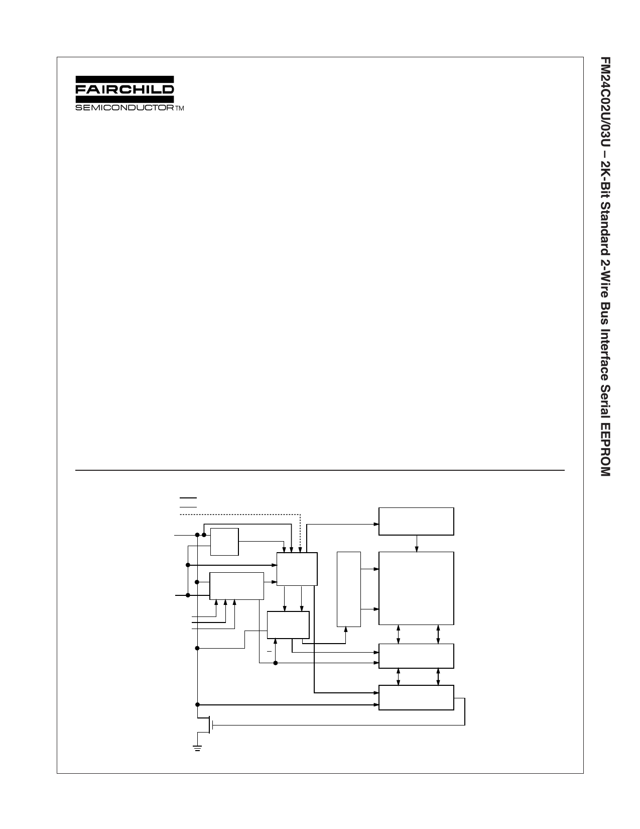
Block Diagram
VCC
VSS
WP
SDA
SCL
A2
A1
A0
START
STOP
LOGIC
SLAVE ADDRESS
REGISTER &
COMPARATOR
CONTROL
LOGIC
WORD
ADDRESS
COUNTER
R/W
XDEC
H.V. GENERATION
TIMING &CONTROL
E2PROM
ARRAY
YDEC
CK
DIN
DATA REGISTER
DOUT
© 2000 Fairchild Semiconductor International
FM24C02U/03U Rev. A.3
1
www.fairchildsemi.com
1 page 
AC Test Conditions
Input Pulse Levels
Input Rise and Fall Times
VCC x 0.1 to VCC x 0.9
10 ns
Input & Output Timing Levels VCC x 0.3 to VCC x 0.7
Output Load
1 TTL Gate and CL = 100 pF
AC Testing Input/Output Waveforms
0.9VCC
0.1VCC
0.7VCC
0.3VCC
Read and Write Cycle Limits (Standard and Low VCC Range 2.7V - 5.5V)
Symbol
Parameter
100 KHz
Min Max
400 KHz
Min Max
fSCL SCL Clock Frequency
TI Noise Suppression Time Constant at
SCL, SDA Inputs (Minimum VIN
Pulse width)
100
100
400
50
tAA SCL Low to SDA Data Out Valid 0.3 3.5 0.1 0.9
tBUF Time the Bus Must Be Free before
a New Transmission Can Start
4.7
1.3
tHD:STA
tLOW
tHIGH
tSU:STA
Start Condition Hold Time
Clock Low Period
Clock High Period
Start Condition Setup Time
(for a Repeated Start Condition)
4.0
4.7
4.0
4.7
0.6
1.5
0.6
0.6
tHD:DAT
tSU:DAT
tR
tF
tSU:STO
tDH
tWR
(Note 4)
Data in Hold Time
Data in Setup Time
SDA and SCL Rise Time
SDA and SCL Fall Time
Stop Condition Setup Time
Data Out Hold Time
Write Cycle Time
4.5V to 5.5V VCC
2.7V to 4.5V VCC
00
250 100
1 0.3
300 300
4.7 0.6
300 50
10 10
15 15
Units
KHz
ns
µs
µs
µs
µs
µs
µs
ns
ns
µs
ns
µs
ns
ms
Note 4: The write cycle time (tWR) is the time from a valid stop condition of a write sequence to the end of the internal erase/program cycle. During the write cycle, the
FM24C02U/03U bus interface circuits are disabled, SDA is allowed to remain high per the bus-level pull-up resistor, and the device does not respond to its slave address. Refer
"Write Cycle Timing" diagram.
Bus Timing
tF
tLOW
SCL
SDA
tSU:STA
tHD:STA
;;IN
SDA
OUT
tAA
tHIGH
tHD:DAT
tR
tLOW
tSU:DAT
tDH
tSU:STO
tBUF
FM24C02U/03U Rev. A.3
5
www.fairchildsemi.com
5 Page 
Write Operations
BYTE WRITE
For a write operation, a second address field is required which is a
word address that is comprised of eight bits and provides access to
any one of the 256 bytes in the selected page of memory. Upon
receipt of the byte address, the FM24C02U/03U responds with an
acknowledge and waits for the next eight bits of data, again,
responding with an acknowledge. The master then terminates the
transfer by generating a stop condition at which time the FM24C02U/
03U begins the internal write cycle to the nonvolatile memory. While
the internal write cycle is in progress, the FM24C02U/03U inputs
are disabled, and the device will not respond to any requests from
the master for the duration of tWR. Refer to Figure 4 for the address,
acknowledge, and data transfer sequence.
PAGE WRITE
To minimize write cycle time, FM24C02U/03U offer Page Write
feature, by which, up to a maximum of 16 contiguous byte
locations can be programmed all at once (instead of 16 individual
byte writes). To facilitate this feature, the memory array is orga-
nized in terms of “Pages.” A Page consists of 16 contiguous byte
locations starting at every 16-Byte address boundary (for ex-
ample, starting at array address 0x00, 0x10, 0x20 etc.). Page
Write operation limits access to byte locations within a page. In
other words a single Page Write operation will not cross over to
locations on another page but will “roll over” to the beginning of the
page whenever end of Page is reached and additional locations
are continued to be accessed. A Page Write operation can be
initiated to begin at any location within a page (starting address of
the Page Write operation need not be the starting address of a
Page).
Page Write is initiated in the same manner as the Byte Write
operation; but instead of terminating the cycle after transmitting
the first data byte, the master can further transmit up to 15 more
bytes. After the receipt of each byte, FM24C02U/03U will respond
with an acknowledge pulse, increment the internal address counter
to the next address, and is ready to accept the next data. If the
master should transmit more than sixteen bytes prior to generat-
ing the STOP condition, the address counter will “roll over” and
previously written data will be overwritten. As with the Byte Write
operation, all inputs are disabled until completion of the internal
write cycle. Refer to Figure 5 for the address, acknowledge, and
data transfer sequence.
Acknowledge Polling
Once the stop condition is issued to indicate the end of the host’s
write operation, the FM24C02U/03U initiates the internal write
cycle. ACK polling can be initiated immediately. This involves
issuing the start condition followed by the slave address for a write
operation. If the FM24C02U/03U is still busy with the write
operation, no ACK will be returned. If the FM24C02U/03U has
completed the write operation, an ACK will be returned and the
host can then proceed with the next read or write operation.
Write Protection (FM24C03U Only)
Programming of the upper half (upper 1Kbit) of the memory will not
take place if the WP pin of the FM24C03U is connected to VCC.
The FM24C03U will respond to slave and byte addresses; but if
the memory accessed is write protected by the WP pin, the
FM24C03U will not generate an acknowledge after the first byte
of data has been received. Thus, the program cycle will not be
started when the stop condition is asserted.
Byte Write (Figure 4)
Bus Activity:
Master
SDA Line
Bus Activity:
EEPROM
S
T
A SLAVE
R ADDRESS
T
A
C
K
WORD
ADDRESS
A
C
K
DATA
S
T
O
P
A
C
K
Page Write (Figure 5)
Bus Activity:
Master
SDA Line
S
T
A SLAVE
R ADDRESS
T
Bus Activity:
EEPROM
WORD ADDRESS (n)
AA
CC
KK
DATA n
DATA n + 1
AA
CC
KK
DATA n + 15
S
T
O
P
A
C
K
FM24C02U/03U Rev. A.3
11
www.fairchildsemi.com
11 Page | ||
| Páginas | Total 14 Páginas | |
| PDF Descargar | [ Datasheet FM24C02U.PDF ] | |
Hoja de datos destacado
| Número de pieza | Descripción | Fabricantes |
| FM24C02 | 4K-Bit Standard 2-Wire Bus Interface Serial EEPROM | Fairchild Semiconductor |
| FM24C02 | 2-Wire Serial EEPROM | Fudan |
| FM24C02A | 2-Wire Serial EEPROM | Fudan |
| FM24C02B | 2-Wire Serial EEPROM | Fudan |
| Número de pieza | Descripción | Fabricantes |
| SLA6805M | High Voltage 3 phase Motor Driver IC. |
Sanken |
| SDC1742 | 12- and 14-Bit Hybrid Synchro / Resolver-to-Digital Converters. |
Analog Devices |
|
DataSheet.es es una pagina web que funciona como un repositorio de manuales o hoja de datos de muchos de los productos más populares, |
| DataSheet.es | 2020 | Privacy Policy | Contacto | Buscar |