|
|
|
PDF AT93C66A-10SE-2.7 Data sheet ( Hoja de datos )
| Número de pieza | AT93C66A-10SE-2.7 | |
| Descripción | 3-wire Serial EEPROMs 2K (256 x 8 or 128 x 16) | |
| Fabricantes | ATMEL Corporation | |
| Logotipo | ||
Hay una vista previa y un enlace de descarga de AT93C66A-10SE-2.7 (archivo pdf) en la parte inferior de esta página. Total 18 Páginas | ||
|
No Preview Available !
Features
• Low-voltage and Standard-voltage Operation
– 2.7 (VCC = 2.7V to 5.5V)
– 1.8 (VCC = 1.8V to 5.5V)
• User-selectable Internal Organization
– 2K: 256 x 8 or 128 x 16
– 4K: 512 x 8 or 256 x 16
• 3-wire Serial Interface
• Sequential Read Operation
• 2 MHz Clock Rate (5V)
• Self-timed Write Cycle (10 ms Max)
• High Reliability
– Endurance: 1 Million Write Cycles
– Data Retention: 100 Years
• Automotive Grade, Extended Temperature, and Lead-free/Halogen-free
Devices Available
• 8-lead PDIP, 8-lead JEDEC SOIC, 8-lead EIAJ SOIC, 8-lead MAP, 8-lead TSSOP,
and 8-ball dBGA2™ Packages
3-wire Serial
EEPROMs
2K (256 x 8 or 128 x 16)
4K (512 x 8 or 256 x 16)
Description
The AT93C56A/66A provides 2048/4096 bits of serial electrically erasable program-
mable read-only memory (EEPROM) organized as 128/256 words of 16 bits each
when the ORG pin is connected to VCC and 256/512 words of 8 bits each when it is
tied to ground. The device is optimized for use in many industrial and commercial
applications where low-power and low-voltage operations are essential. The
AT93C56A/66A is available in space-saving 8-lead PDIP, 8-lead JEDEC SOIC, 8-lead
EIAJ SOIC, 8-lead MAP, 8-lead TSSOP, and 8-ball dBGA2™ packages.
AT93C56A
AT93C66A
Advance
Information
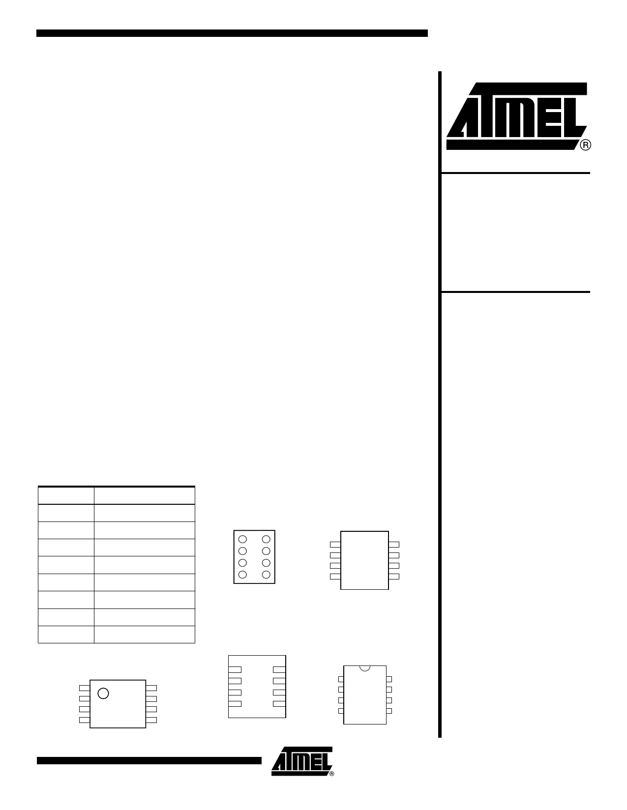
Pin Configurations
Pin Name
CS
SK
DI
DO
GND
VCC
ORG
DC
Function
Chip Select
Serial Data Clock
Serial Data Input
Serial Data Output
Ground
Power Supply
Internal Organization
Don’t Connect
8-lead TSSOP
CS 1
SK 2
DI 3
DO 4
8 VCC
7 DC
6 ORG
5 GND
8-ball dBGA2
VCC
DC
ORG
GND
8
7
6
5
1 CS
2 SK
3 DI
4 DO
Bottom View
8-lead SOIC
CS 1
SK 2
DI 3
DO 4
8 VCC
7 DC
6 ORG
5 GND
8-lead MAP
VCC 8
DC 7
ORG 6
GND 5
1 CS
2 SK
3 DI
4 DO
Bottom View
8-lead PDIP
CS 1
SK 2
DI 3
DO 4
8 VCC
7 DC
6 ORG
5 GND
Rev. 3378F–SEEPR–04/04
1
1 page 
Instruction Set for the AT93C56A and AT93C66A
Op
Instruction SB Code
Address
x 8 x 16
Data
x 8 x 16
READ
1 10
A8 – A0
A7 – A0
EWEN
ERASE
WRITE
ERAL
1 00 11XXXXXXX 11XXXXXX
1 11
1 01
A8 – A0
A8 – A0
A7 – A0
A7 – A0
D7 – D0
D15 – D0
1 00 10XXXXXXX 10XXXXXX
WRAL
1 00 01XXXXXXX 01XXXXXX D7 – D0 D15 – D0
EWDS
1 00 00XXXXXXX 00XXXXXX
Note: The X’s in the address field represent don’t care values and must be clocked.
Comments
Reads data stored in memory, at
specified address.
Write enable must precede all
programming modes.
Erases memory location An – A0.
Writes memory location An – A0.
Erases all memory locations. Valid
only at VCC = 4.5V to 5.5V.
Writes all memory locations. Valid
only at VCC = 5.0V ±10% and Disable
Register cleared.
Disables all programming instructions.
Functional Description
The AT93C56A/66A is accessed via a simple and versatile 3-wire serial communication
interface. Device operation is controlled by seven instructions issued by the host pro-
cessor. A valid instruction starts with a rising edge of CS and consists of a Start Bit
(logic “1”) followed by the appropriate Op Code and the desired memory address
location.
READ (READ): The Read (READ) instruction contains the address code for the mem-
ory location to be read. After the instruction and address are decoded, data from the
selected memory location is available at the serial output pin DO. Output data changes
are synchronized with the rising edges of serial clock SK. It should be noted that a
dummy bit (logic “0”) precedes the 8- or 16-bit data output string. The AT93C56A/66A
supports sequential read operations. The device will automatically increment the inter-
nal address pointer and clock out the next memory location as long as Chip Select (CS)
is held high. In this case, the dummy bit (logic “0”) will not be clocked out between mem-
ory locations, thus allowing for a continuous stream of data to be read.
ERASE/WRITE (EWEN): To assure data integrity, the part automatically goes into the
Erase/Write Disable (EWDS) state when power is first applied. An Erase/Write Enable
(EWEN) instruction must be executed first before any programming instructions can be
carried out. Please note that once in the EWEN state, programming remains enabled
until an EWDS instruction is executed or VCC power is removed from the part.
ERASE (ERASE): The Erase (ERASE) instruction programs all bits in the specified
memory location to the logical “1” state. The self-timed erase cycle starts once the
ERASE instruction and address are decoded. The DO pin outputs the READY/BUSY
status of the part if CS is brought high after being kept low for a minimum of 250 ns (tCS).
A logic “1” at pin DO indicates that the selected memory location has been erased, and
the part is ready for another instruction.
3378F–SEEPR–04/04
5
5 Page 
AT93C66A Ordering Information
Ordering Code
Package
Operation Range
AT93C66A-10PI-2.7
8P3
AT93C66A-10SI-2.7
AT93C66AW-10SI-2.7
AT93C66A-10TI-2.7
AT93C66AU3-10UI-2.7
AT93C66AY1-10YI-2.7
8S1
8S2
8A2
8U3-1
8Y1
Industrial
(−40°C to 85°C)
AT93C66A-10PI-1.8
AT93C66A-10SI-1.8
AT93C66AW-10SI-1.8
AT93C66A-10TI-1.8
AT93C66AU3-10UI-1.8
AT93C66AY1-10YI-1.8
8P3
8S1
8S2
8A2
8U3-1
8Y1
Industrial
(−40°C to 85°C)
AT93C66A-10SU-2.7
AT93C66A-10SU-1.8
AT93C66A-10TU-2.7
AT93C66A-10TU-1.8
8S1
8S1
Lead-free/Halogen-free/
Industrial Temperature
8A2 (−40°C to 85°C)
8A2
AT93C66A-10SQ-2.7
Lead-free/Halogen-free/
8S1 High Grade/Extended Temperature
(−40°C to 125°C)
AT93C66A-10SE-2.7
High Grade/Extended Temperature
8S1 (−40°C to 125°C)
Note: For 2.7V devices used in the 4.5V to 5.5V range, please refer to performance values in the AC and DC characteristics table.
8P3
8S1
8S2
8A2
8U3-1
8Y1
−2.7
−1.8
Package Type
8-lead, 0.300" Wide, Plastic Dual Inline Package (PDIP)
8-lead, 0.150" Wide, Plastic Gull Wing Small Outline (JEDEC SOIC)
8-lead, 0.200" Wide, Plastic Gull Wing Small Outline (EIAJ SOIC)
8-lead, 0.170" Wide, Thin Shrink Small Outline Package (TSSOP)
8-ball, die Ball Grid Array Package (dBGA2)
8-lead, 4.90 mm x 3.00 mm Body, Dual Footprint, Non-leaded, Miniature Array Package (MAP)
Options
Low-voltage (2.7V to 5.5V)
Low-voltage (1.8V to 5.5V)
3378F–SEEPR–04/04
11
11 Page | ||
| Páginas | Total 18 Páginas | |
| PDF Descargar | [ Datasheet AT93C66A-10SE-2.7.PDF ] | |
Hoja de datos destacado
| Número de pieza | Descripción | Fabricantes |
| AT93C66A-10SE-2.7 | 3-wire Serial EEPROMs 2K (256 x 8 or 128 x 16) | ATMEL Corporation |
| Número de pieza | Descripción | Fabricantes |
| SLA6805M | High Voltage 3 phase Motor Driver IC. |
Sanken |
| SDC1742 | 12- and 14-Bit Hybrid Synchro / Resolver-to-Digital Converters. |
Analog Devices |
|
DataSheet.es es una pagina web que funciona como un repositorio de manuales o hoja de datos de muchos de los productos más populares, |
| DataSheet.es | 2020 | Privacy Policy | Contacto | Buscar |