|
|
|
PDF 5962R9582401VQC Data sheet ( Hoja de datos )
| Número de pieza | 5962R9582401VQC | |
| Descripción | Radiation Hardened 8-Bit CMOS Microprocessor | |
| Fabricantes | Intersil Corporation | |
| Logotipo | ||
Hay una vista previa y un enlace de descarga de 5962R9582401VQC (archivo pdf) en la parte inferior de esta página. Total 19 Páginas | ||
|
No Preview Available !
HS-80C85RH
February 1996
Radiation Hardened
8-Bit CMOS Microprocessor
Features
• Devices QML Qualified in Accordance With
MIL-PRF-38535
• Detailed Electrical and Screening Requirements are
Contained in SMD# 5962-95824 and Intersil’ QM Plan
• Radiation Hardened EPI-CMOS
- Parametrics Guaranteed 1 x 10⁵ RAD(Si)
- Transient Upset > 1 x 10⁸ RAD(Si)/s
- Latch-up Free > 1 x 10¹² RAD(Si)/s
• Low Standby Current 500µA Max
• Low Operating Current 5.0mA/MHz (X1 Input)
• Electrically Equivalent to Sandia SA 3000
• 100% Software Compatible with INTEL 8085
• Operation from DC to 2MHz, Post Radiation
• Single 5 Volt Power Supply
• On-Chip Clock Generator and System Controller
• Four Vectored Interrupt Inputs
• Completely Static Design
• Self Aligned Junction Isolated (SAJI) Process
• Military Temperature Range -55oC to +125oC
Description
The HS-80C85RH is an 8-bit CMOS microprocessor fabri-
cated using the Intersil radiation hardened self-aligned junc-
tion isolated (SAJI) silicon gate technology. Latch-up free
operation is achieved by the use of epitaxial starting material
to eliminate the parasitic SCR effect seen in conventional
bulk CMOS devices.
The HS-80C85RH is a functional logic emulation of the
HMOS 8085 and its instruction set is 100% software com-
patible with the HMOS device. The HS80C85RH is designed
for operation with a single 5 volt power supply. Its high level
of integration allows the construction of a radiation hardened
microcomputer system with as few as three ICs (HS-
80C85RH CPU, HS83C55RH ROM I/O, and the HS-81C55/
56RH RAM I/O.
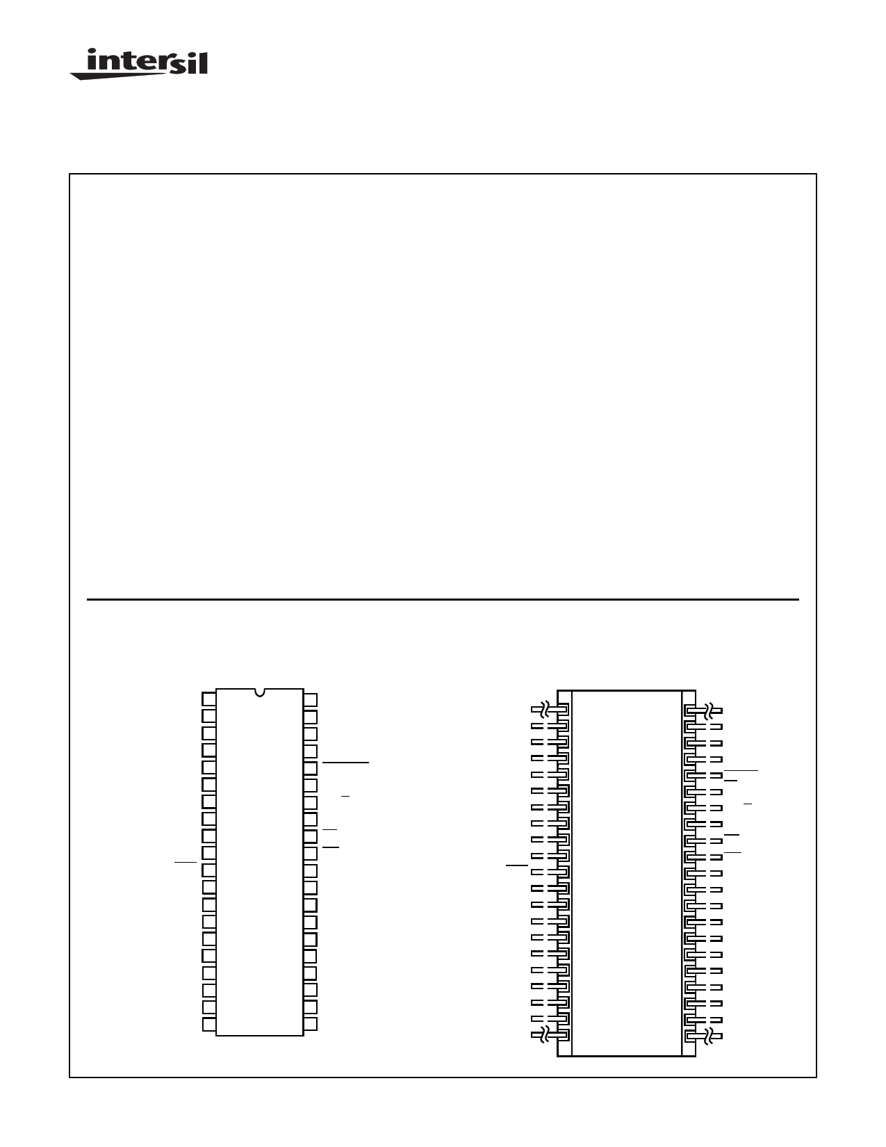
Pinouts
40 LEAD CERAMIC DUAL-IN-LINE
METAL SEAL PACKAGE (SBDIP)
MIL-STD-1835, CDIP2-T40
TOP VIEW
X1 1
X2 2
RESET OUT 3
SOD 4
SID 5
TRAP 6
RST 7.5 7
RST 6.5 8
RST 5.5 9
INTR 10
INTA 11
AD0 12
AD1 13
AD2 14
AD3 15
AD4 16
AD5 17
AD6 18
AD7 19
GND 20
40 VDD
39 HOLD
38 HLDA
37 CLOCK OUT
36 RESET IN
35 READY
34 IO / M
33 S1
32 RD
31 WR
30 ALE
29 S0
28 A15
27 A14
26 A13
25 A12
24 A11
23 A10
22 A9
21 A8
42 LEAD CERAMIC METAL SEAL
FLATPACK PACKAGE (FLATPACK)
INTERSIL OUTLINE K42.A
TOP VIEW
X1
X2
RESET
OUT
SOD
SID
TRAP
RST 7.5
RST 6.5
RST 5.5
INTR
INTA
AD0
AD1
AD2
AD3
AD4
NC
NC
AD5
AD6
AD7
1
2
3
4
5
6
7
8
9
10
11
12
13
14
15
16
17
18
19
20
21
42 VDD
41 HOLD
40 HLDA
39 CLOCK
OUT
38 RESET
37
IN
READY
36 IO / M
35 S1
34 RD
33 WR
32 ALE
31 S0
30 A15
29 A14
28 A13
27 A12
26 A11
25 A10
24 A9
23 A8
22 GND
CAUTION: These devices are sensitive to electrostatic discharge; follow proper IC Handling Procedures.
http://www.intersil.com or 407-727-9207 | Copyright © Intersil Corporation 1999
1
Spec Number 518054
File Number 3036.2
1 page 
Specifications HS-80C85RH
Absolute Maximum Ratings
Reliability Information
Supply Voltage . . . . . . . . . . . . . . . . . . . . . . . . . . . . . . . . . . . . . +7.0V
Input, Output or I/O Voltage . . . . . . . . . . . . GND-0.3V to VCC+0.3V
Storage Temperature Range . . . . . . . . . . . . . . . . . -65oC to +150oC
Junction Temperature . . . . . . . . . . . . . . . . . . . . . . . . . . . . . . +175oC
Lead Temperature (Soldering 10s) . . . . . . . . . . . . . . . . . . . . +300oC
Typical Derating Factor. . . . . . . . . . .2.0mA/MHz Increase in IDDOP
ESD Classification . . . . . . . . . . . . . . . . . . . . . . . . . . . . . . . . Class 1
Thermal Resistance
θJA θJC
SBDIP Package. . . . . . . . . . . . . . . . . . . . 45oC/W 10oC/W
Ceramic Flatpack Package . . . . . . . . . . . 77oC/W 13oC/W
Maximum Package Power Dissipation at +125oC Ambient
SBDIP Package. . . . . . . . . . . . . . . . . . . . . . . . . . . . . . . . . . 1.11W
Ceramic Flatpack Package . . . . . . . . . . . . . . . . . . . . . . . . . 0.65W
If device power exceeds package dissipation capability, provide heat
sinking or derate linearly at the following rate:
SBDIP Package. . . . . . . . . . . . . . . . . . . . . . . . . . . . . . 22.2mW/oC
Ceramic Flatpack Package . . . . . . . . . . . . . . . . . . . . . 13.0mW/oC
CAUTION: Stresses above those listed in “Absolute Maximum Ratings” may cause permanent damage to the device. This is a stress only rating and operation
of the device at these or any other conditions above those indicated in the operational sections of this specification is not implied.
Operating Conditions
Operating Supply Voltage Range (VDD) . . . . . . . +4.75V to +5.25V
Operating Temperature Range (TA) . . . . . . . . . . . . -55oC to +125oC
Input Low Voltage . . . . . . . . . . . . . . . . . . . . . . . . . . . . . .0V to +0.8V
Input High Voltage. . . . . . . . . . . . . . . . . . . . . . . . VDD -0.5V to VDD
TABLE 1. DC ELECTRICAL PERFORMANCE CHARACTERISTICS
PARAMETER
Input Leakage
Current
High Level Output
Voltage
Low Level Output
Voltage
Static Current
Operating Supply
Current (Note 2)
Functional Tests
SYMBOL
IIH or
IIL
VOH
VOL
IDDSB
IDDOP
FT
CONDITIONS
GROUP A
SUBGROUPS
VDD = 5.25V, VI = VDD
or GND
1, 2, 3
VDD = 4.75V, IOH = -1.0mA
1, 2, 3
VDD = 5.25V, IOL = 1.0mA,
1, 2, 3
VDD = 5.25V, Clock Out = Hi
and Low
VDD = 5.25V, f = 1MHz
(Note 2)
VDD = 4.75V and 5.25V,
TCYC = 500ns,
VOL ≤ VDD/2, VOH ≥ VDD/2
1, 2, 3
1, 2, 3
7, 8A, 8B
TEMPERATURE
-55oC, +25oC, or
+125oC
-55oC, +25oC, or
+125oC
-55oC, +25oC, or
+125oC
-55oC, +25oC, or
+125oC
-55oC, +25oC, or
+125oC
-55oC, +25oC, or
+125oC
NOTES:
1. All devices guaranteed at worst case limits and over radiation.
2. Operating supply current (IDDOP) is proportional to crystal frequency. Parts are tested at 1MHz
LIMITS
MIN MAX
-1.0 1.0
VDD -0.5
-
- 0.5
- 500
- 5.0
--
UNITS
µA
V
V
µA
mA/MHz
-
TABLE 2. AC ELECTRICAL PERFORMANCE CHARACTERISTICS
PARAMETER
CLK Low Time (Standard CLK Loading)
CLK High Time (Standard CLK Loading)
CLK Rise Time
CLK Fall Time
X1 Rising to CLK Rising
X1 Rising to CLK Falling
A8-15 Valid to Leading Edge of Control (Note 5)
A0-7 Valid to Leading Edge of Control
A0-15 Valid to Valid Data In
Address Float After Leading Edge of READ
(INTA)
GROUP A
SYMBOL SUBGROUPS
T1 9, 10, 11
T2 9, 10, 11
Tr 9, 10, 11
Tf 9, 10, 11
TXKR
9, 10, 11
TXKF
9, 10, 11
TAC
9, 10, 11
TACL
9, 10, 11
TAD
9, 10, 11
TAFR
9, 10, 11
TEMPERATURE
-55oC, +25oC, +125oC
-55oC, +25oC, +125oC
-55oC, +25oC, +125oC
-55oC, +25oC, +125oC
-55oC, +25oC, +125oC
-55oC, +25oC, +125oC
-55oC, +25oC, +125oC
-55oC, +25oC, +125oC
-55oC, +25oC, +125oC
-55oC, +25oC, +125oC
LIMITS
MIN MAX
40 -
100 -
- 115
- 115
30 250
50 275
300 -
300 -
875 -
- 70
UNITS
ns
ns
ns
ns
ns
ns
ns
ns
ns
ns
Spec Number 518054
5
5 Page 
HS-80C85RH
TABLE 9. INSTRUCTION SET SUMMARY (Continued)
INSTRUCTION CODE
MNEMONIC D7 D6 D5 D4 D3 D2 D1 D0
OPERATIONS
DESCRIPTION
JPE 1 1 1 0 1 0 1 0 Jump on parity
even
INSTRUCTION CODE
MNEMONIC D7 D6 D5 D4 D3 D2 D1 D0
OPERATIONS
DESCRIPTION
ADC M
1 0 0 0 1 1 1 0 Add memory to A
with carry
JPO
PCHL
1 1 1 0 0 0 1 0 Jump on parity odd
1 1 1 0 1 0 0 1 H & L to program
counter
ADl
ACl
1 1 0 0 0 1 1 0 Add immediate to A
1 1 0 0 1 1 1 0 Add immediate to A
with carry
CALL
DAD B
0 0 0 0 1 0 0 1 Add B & C to H & L
CALL
CC
1 1 0 0 1 1 0 1 Call unconditional
1 1 0 1 1 1 0 0 Call on carry
DAD D
DAD H
0 0 0 1 1 0 0 1 Add D & E to H & L
0 0 1 0 1 0 0 1 Add H & L to H & L
CNC
LOGICAL
ANA r
XRA r
ORA r
CMP r
ANA M
XRA M
ORA M
CMP M
ANI
XRI
ORl
CPl
1 1 0 1 0 1 0 0 Call on no carry
1 0 1 0 0 S S S And register with A
1 0 1 0 1 S S S Exclusive OR
register with A
1 0 1 1 0 S S S OR register with A
1 0 1 1 1 S S S Compare register
with A
1 0 1 0 0 1 1 0 And memory with A
1 0 1 0 1 1 1 0 Exclusive OR mem-
ory with A
1 0 1 1 0 1 1 0 OR memory with A
1 0 1 1 1 1 1 0 Compare memory
with A
1 1 1 0 0 1 1 0 And immediate
with A
1 1 1 0 1 1 1 0 Exclusive OR
immediate with A
1 1 1 1 0 1 1 0 OR immediate
with A
1 1 1 1 1 1 1 0 Compare immedi-
ate with A
DAD SP
SUBTRACT
SUB r
SBB r
SUB M
SBB M
SUl
SBl
SPECIALS
CMA
STC
CMC
DAA
CONTROL
0 0 1 1 1 0 0 1 Add stack pointer to
H&L
1 0 0 1 0 S S S Subtract register
from A
1 0 0 1 1 S S S Subtract register
from A with borrow
1 0 0 1 0 1 1 0 Subtract memory
from A
1 0 0 1 1 1 1 0 Subtract memory
from A with borrow
1 1 0 1 0 1 1 0 Subtract immedi-
ate from A
1 1 0 1 1 1 1 0 Subtract immedi-
ate from A with
borrow
0 0 1 0 1 1 1 1 Complement A
0 0 1 1 0 1 1 1 Set carry
0 0 1 1 1 1 1 1 Complement carry
0 0 1 0 0 1 1 1 Decimal adjust A
ROTATE
RLC
0 0 0 0 0 1 1 1 Rotate A left
El
DI
1 1 1 1 1 0 1 1 Enable Interrupts
1 1 1 1 0 0 1 1 Disable Interrupt
RRC
0 0 0 0 1 1 1 1 Rotate A right
NOP
0 0 0 0 0 0 0 0 No-operation
RAL
RAR
INX H
DCX B
DCX D
0 0 0 1 0 1 1 1 Rotate A left
through carry
0 0 0 1 1 1 1 1 Rotate A right
through carry
0 0 1 0 0 0 1 1 Increment H & L
registers
0 0 0 0 1 0 1 1 Decrement B & C
0 0 0 1 1 0 1 1 Decrement D & E
HLT 0 1 1 1 0 1 1 0 Halt
RIM 0 0 1 0 0 0 0 0 Read Interrupt
Mask
SlM 0 0 1 1 0 0 0 0 Set Interrupt Mask
NOTES:
1. DDS or SSS: B000, C001, D010, E011, H100, L101, Memory 110, A111
2. Two possible cycle times (6/12) indicate instruction cycles dependent on condi-
tion flags.
DCX H
ADD
0 0 1 0 1 0 1 1 Decrement H & L
† All mnemonics copyrighted „ Intel Corporation 1976
ADD r
1 0 0 0 0 S S S Add register to A
ADC r
ADD M
1 0 0 0 1 S S S Add register to A
with carry
1 0 C 0 0 1 1 0 Add memory to A
Spec Number 518054
11
11 Page | ||
| Páginas | Total 19 Páginas | |
| PDF Descargar | [ Datasheet 5962R9582401VQC.PDF ] | |
Hoja de datos destacado
| Número de pieza | Descripción | Fabricantes |
| 5962R9582401VQC | Radiation Hardened 8-Bit CMOS Microprocessor | Intersil Corporation |
| Número de pieza | Descripción | Fabricantes |
| SLA6805M | High Voltage 3 phase Motor Driver IC. |
Sanken |
| SDC1742 | 12- and 14-Bit Hybrid Synchro / Resolver-to-Digital Converters. |
Analog Devices |
|
DataSheet.es es una pagina web que funciona como un repositorio de manuales o hoja de datos de muchos de los productos más populares, |
| DataSheet.es | 2020 | Privacy Policy | Contacto | Buscar |