|
|
|
PDF 74AC138 Data sheet ( Hoja de datos )
| Número de pieza | 74AC138 | |
| Descripción | 3 TO 8 LINE DECODER INVERTING | |
| Fabricantes | STMicroelectronics | |
| Logotipo | ||
Hay una vista previa y un enlace de descarga de 74AC138 (archivo pdf) en la parte inferior de esta página. Total 10 Páginas | ||
|
No Preview Available !
74AC138
3 TO 8 LINE DECODER (INVERTING)
s HIGH SPEED: tPD = 4.5ns (TYP.) at VCC = 5V
s LOW POWER DISSIPATION:
ICC = 4µA(MAX.) at TA=25°C
s HIGH NOISE IMMUNITY:
VNIH = VNIL = 28 % VCC (MIN.)
s 50Ω TRANSMISSION LINE DRIVING
CAPABILITY
s SYMMETRICAL OUTPUT IMPEDANCE:
|IOH| = IOL = 24mA (MIN)
s BALANCED PROPAGATION DELAYS:
tPLH ≅ tPHL
s OPERATING VOLTAGE RANGE:
VCC (OPR) = 2V to 6V
s PIN AND FUNCTION COMPATIBLE WITH
74 SERIES 138
s IMPROVED LATCH-UP IMMUNITY
DESCRIPTION
The 74AC138 is an advanced high-speed CMOS
3 TO 8 LINE DECODER (INVERTING) fabricated
with sub-micron silicon gate and double-layer
metal wiring C2MOS tecnology.
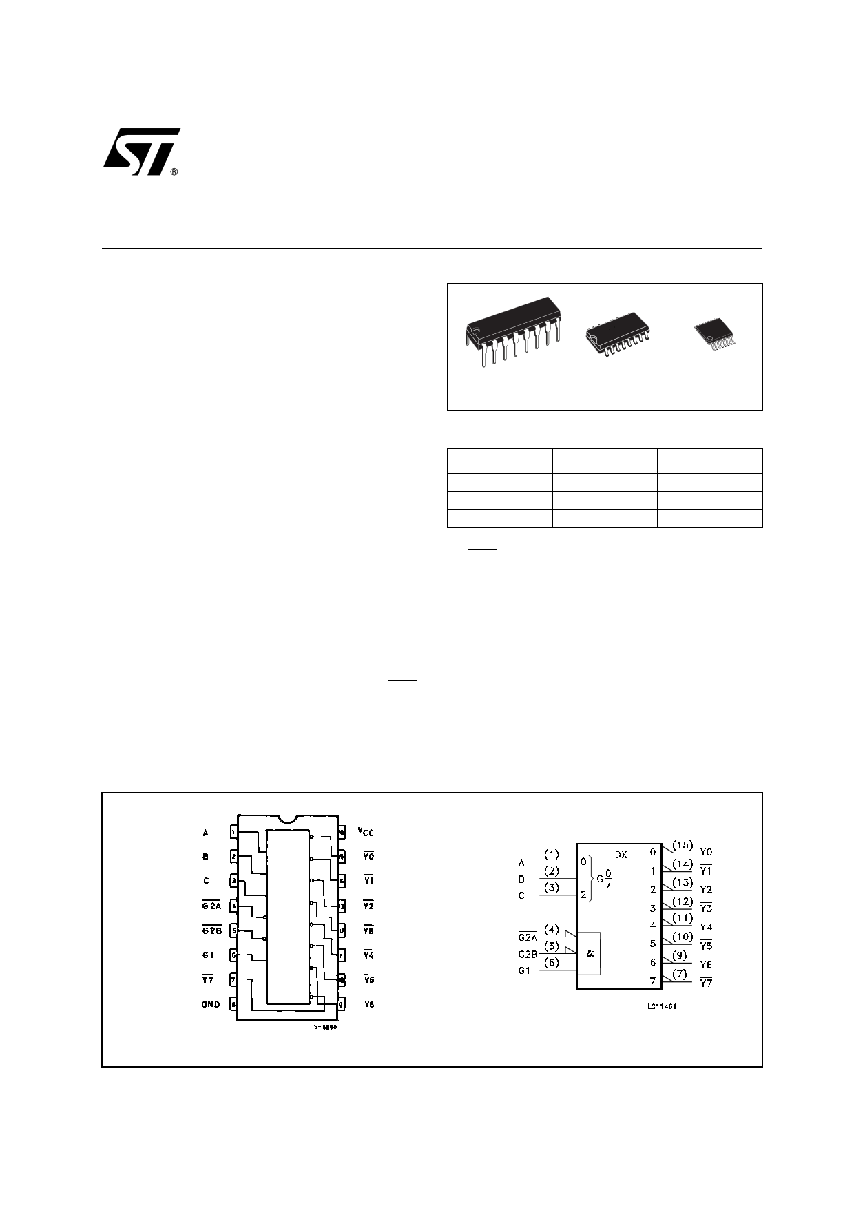
If the device is enabled, 3 binary select inputs (A,
B, and C) determine which one of the outputs will
go low. If enable input G1 is held low or either G2A
DIP
SOP
TSSOP
ORDER CODES
PACKAGE
DIP
SOP
TSSOP
TUBE
74AC138B
74AC138M
T&R
74AC138MTR
74AC138TTR
or G2B is held high, the decoding function is
inhibited and all the 8 outputs go to high.
Tree enable inputs are provided to ease cascade
connection and application of address decoders
for memory systems.
All inputs and outputs are equipped with
protection circuits against static discharge, giving
them 2KV ESD immunity and transient excess
voltage.
PIN CONNECTION AND IEC LOGIC SYMBOLS
April 2001
1/10
1 page 
74AC138
AC ELECTRICAL CHARACTERISTICS (CL = 50 pF, RL = 500 Ω, Input tr = tf = 3ns)
Test Condition
Value
Symbol
Parameter
VCC
(V)
tPLH tPHL Propagation Delay
Time
A, B, C to Y
tPLH tPHL Propagation Delay
Time
G1 to Y
tPLH tPHL Propagation Delay
Time
G2A or G2B to Y
3.3(*)
5.0(**)
3.3(*)
5.0(**)
3.3(*)
5.0(**)
TA = 25°C
-40 to 85°C -55 to 125°C Unit
Min. Typ. Max. Min. Max. Min. Max.
1.5 5.5 10.5 1.5 14.0 1.5 15.4
ns
1.5 4.5 9.0 1.5 10.0 1.5 11.0
1.5 6.0 10.5 1.5 14.0 1.5 15.4
ns
1.5 4.5 11.0 1.5 10.0 1.5 11.0
1.5 5.5 10.5 1.5 12.7 1.5 14.0
ns
1.5 4.5 9.0 1.5 10.0 1.5 10.0
(*) Voltage range is 3.3V ± 0.3V
(**) Voltage range is 5.0V ± 0.5V
CAPACITIVE CHARACTERISTICS
Test Condition
Value
Symbol
Parameter
VCC
(V)
TA = 25°C
-40 to 85°C -55 to 125°C Unit
Min. Typ. Max. Min. Max. Min. Max.
CIN Input Capacitance 5.0
4
pF
CPD Power Dissipation 5.0
Capacitance
(note 1)
fIN = 10MHz
60
pF
1) CPD is defined as the value of the IC’s internal equivalent capacitance which is calculated from the operating current consumption without
load. (Refer to Test Circuit). Average operating current can be obtained by the following equation. ICC(opr) = CPD x VCC x fIN + ICC/n (per circuit)
TEST CIRCUIT
CL = 50pF or equivalent (includes jig and probe capacitance)
RL = R1 = 500Ω or equivalent
RT = ZOUT of pulse generator (typically 50Ω)
5/10
5 Page | ||
| Páginas | Total 10 Páginas | |
| PDF Descargar | [ Datasheet 74AC138.PDF ] | |
Hoja de datos destacado
| Número de pieza | Descripción | Fabricantes |
| 74AC132 | Quad 2-Input NAND Schmitt Trigger | ON Semiconductor |
| 74AC138 | 3 TO 8 LINE DECODER INVERTING | STMicroelectronics |
| 74AC138 | 1-of-8 Decoder/Demultiplexer | Fairchild Semiconductor |
| 74AC138B | 3 TO 8 LINE DECODER INVERTING | STMicroelectronics |
| Número de pieza | Descripción | Fabricantes |
| SLA6805M | High Voltage 3 phase Motor Driver IC. |
Sanken |
| SDC1742 | 12- and 14-Bit Hybrid Synchro / Resolver-to-Digital Converters. |
Analog Devices |
|
DataSheet.es es una pagina web que funciona como un repositorio de manuales o hoja de datos de muchos de los productos más populares, |
| DataSheet.es | 2020 | Privacy Policy | Contacto | Buscar |