|
|
|
PDF JAN1524J Data sheet ( Hoja de datos )
| Número de pieza | JAN1524J | |
| Descripción | REGULATING PULSE WIDTH MODULATOR | |
| Fabricantes | Microsemi Corporation | |
| Logotipo | ||
Hay una vista previa y un enlace de descarga de JAN1524J (archivo pdf) en la parte inferior de esta página. Total 6 Páginas | ||
|
No Preview Available !
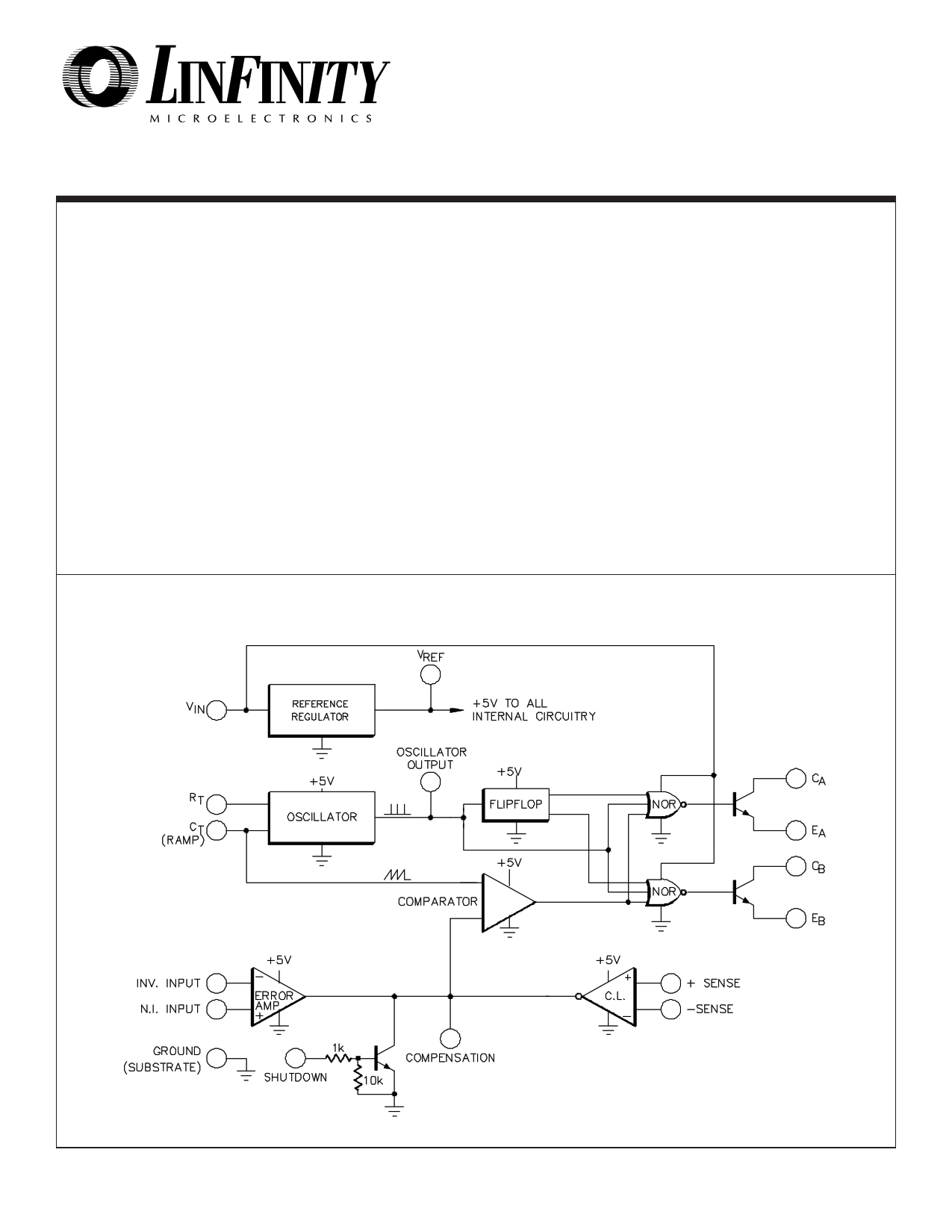
SG1524/SG2524/SG3524
REGULATING PULSE WIDTH MODULATOR
DESCRIPTION
This monolithic integrated circuit contains all the control circuitry for a
regulating power supply inverter or switching regulator. Included in a 16-
pin dual-in-line package is the voltage reference, error amplifier, oscillator,
pulse width modulator, pulse steering flip-flop, dual alternating output
switches and current limiting and shut-down circuitry. This device can be
used for switching regulators of either polarity, transformer coupled DC to
DC converters, transformerless voltage doublers and polarity converters,
as well as other power applications. The SG1524 is specified for operation
over the full military ambient temperature range of -55°C to +125°C, the
SG2524 for -25°C to +85°C, and the SG3524 is designed for commercial
applications of 0°C to +70°C.
FEATURES
• 8V to 40V operation
• 5V reference
• Reference line and load regulation of 0.4%
• Reference temperature coefficient < ± 1%
• 100Hz to 300KHz oscillator range
• Excellent external sync capability
• Dual 50mA output transistors
• Current limit circuitry
• Complete PWM power control circuitry
• Single ended or push-pull outputs
• Total supply current less than 10mA
HIGH RELIABILITY FEATURES - SG1524
♦ Available to MIL-STD-883B and DESC SMD
♦ MIL-M-38510/12601BEA - JAN1524J
♦ Radiation data available
♦ LMI level "S" processing available
BLOCK DIAGRAM
4/90 Rev 1.1 2/94
Copyright © 1994
LINFINITY Microelectronics Inc.
1 11861 Western Avenue ∞ Garden Grove, CA 92841
(714) 898-8121 ∞ FAX: (714) 893-2570
1 page 
APPLICATION NOTES (continued)
SG1524/SG2524/SG3524
CURRENT LIMITING
The current limiting circuitry of the SG1524 is shown in Figure 3.
By matching the base-emitter voltages of Q1 and Q2, and
assuming a negligible voltage drop across R1:
C.L. Threshold = VBE(Q1) + I1• R2 - VBE(Q2) = I1• R2
~ 200 mV
Although this circuit provides a relatively small threshold with a
negligible temperature coefficient, there are some limitations to
its use because of its simplicity.
The most important of these is the limited common-mode voltage
range: ±0.3 volts around ground. This requires sensing in the
ground or return line of the power supply. Also precautions
should be taken to not turn on the parasitic substrate diode of the
integrated circuit, even under transient conditions. A Schottky
clamp diode at Pin 5 may be required in some configurations to
achieve this.
A second factor to consider is that the response time is relatively
slow. The current limit amplifier is internally compensated by R1
, C1 , and Q1, resulting in a roll-off pole at approximately 300 Hz.
A third factor to consider is the bias current of the C.L. Sense
pins. A constant current of approximately 150µA flows out of Pin
4, and a variable current with a range of 0-150µA flows out of Pin
5. As a result, the equivalent source impedance seen by the
current sense pins should be less than 50 ohms to keep the
threshold error less than 5%.
Since the gain of this circuit is relatively low (42 dB), there is a
transition region as the current limit amplifier takes over pulse
width control from the error amplifier. For testing purposes,
threshold is defined as the input voltage required to get 25% duty
cycle (+2 volts at the error amplifier output) with the error amplifier
signaling maximum duty cycle.
APPLICATION NOTE: If the current limit function is not used on
the SG1524, the common-mode voltage range restriction re-
quires both current sense pins to be grounded.
FIGURE 3 - CURRENT LIMITING CIRCUITRY OF THE SG1524
In this conventional single-ended regulator circuit, the two out-
puts of the SG1524 are connected in parallel for effective 0 - 90%
duty-cycle modulation. The use of an output inductor requires
and R-C phase compensation network for loop stability.
Push-pull outputs are used in this transformer-coupled DC-DC
regulating converter. Note that the oscillator must be set at twice
the desired output frequency as the SG1524's internal flip-flop
divides the frequency by 2 as it switches the P.W.M. signal from
one output to the other. Current limiting is done here in the
primary so that the pulse width will be reduced should transformer
saturation occur.
4/90 Rev 1.1 2/94
Copyright © 1994
LINFINITY Microelectronics Inc.
5 11861 Western Avenue ∞ Garden Grove, CA 92841
(714) 898-8121 ∞ FAX: (714) 893-2570
5 Page | ||
| Páginas | Total 6 Páginas | |
| PDF Descargar | [ Datasheet JAN1524J.PDF ] | |
Hoja de datos destacado
| Número de pieza | Descripción | Fabricantes |
| JAN1524J | REGULATING PULSE WIDTH MODULATOR | Microsemi Corporation |
| Número de pieza | Descripción | Fabricantes |
| SLA6805M | High Voltage 3 phase Motor Driver IC. |
Sanken |
| SDC1742 | 12- and 14-Bit Hybrid Synchro / Resolver-to-Digital Converters. |
Analog Devices |
|
DataSheet.es es una pagina web que funciona como un repositorio de manuales o hoja de datos de muchos de los productos más populares, |
| DataSheet.es | 2020 | Privacy Policy | Contacto | Buscar |