|
|
|
PDF XR16C2852CJ Data sheet ( Hoja de datos )
| Número de pieza | XR16C2852CJ | |
| Descripción | 3.3V AND 5V DUART WITH 128-BYTE FIFO | |
| Fabricantes | Exar Corporation | |
| Logotipo | ||
Hay una vista previa y un enlace de descarga de XR16C2852CJ (archivo pdf) en la parte inferior de esta página. Total 42 Páginas | ||
|
No Preview Available !
áç
XR16C2852
APRIL 2002
3.3V AND 5V DUART WITH 128-BYTE FIFO
REV. 2.0.0
GENERAL DESCRIPTION
The XR16C28521 (2852) is a dual universal asyn-
chronous receiver and transmitter (UART). The de-
vice operates at 3.3V and 5V and is pin-to-pin com-
patible to Exar’s ST16C2552 and XR16L2752. The
2852 register set is compatible to the ST16C2552
and the XR16C2752 enhanced features. It supports
the Exar’s enhanced features of 128 bytes of TX and
RX FIFOs, programmable FIFO trigger level and
FIFO level counters, automatic hardware (RTS/CTS)
and software flow control, automatic RS-485 half du-
plex direction control output and a complete modem
interface. Onboard registers provide the user with op-
erational status and data error flags. An internal loop-
back capability allows system diagnotics. Indepen-
dent programmable baud rate generators are provid-
ed in each channel to select data rates up to 3.125
Mbps at 5V. The 2852 is available in the 44-pin PLCC
package.
NOTE: 1 Covered by U.S. Patent #5,649,122 and #5,832,205
APPLICATIONS
• Portable Appliances
• Telecommunication Network Routers
• Ethernet Network Routers
• Cellular Data Devices
• Factory Automation and Process Controls
FEATURES
• Pin-to-pin compatible to Exar’s ST16C2552 and
XR16L2752
• Improved version of PC16C552
• Two independent UART channels
•Register set compatible to 16C550
•Up to 3 Mbps at 5V, and 2 Mbps at 3.3V
•Transmit and Receive FIFOs of 128 bytes
•Programmable TX and RX FIFO Trigger Levels
•Transmit and Receive FIFO Level Counters
•Automatic Hardware (RTS/CTS) Flow Control
•Selectable Auto RTS Flow Control Hysteresis
•Automatic Software (Xon/Xoff) Flow Control
•Automatic RS-485 Half-duplex Direction Control
Output
•Wireless Infrared (IrDA 1.0) Encoder/Decoder
•Automatic sleep mode
•Full modem interface
• Alternate Function Register
• Device Identification and Revision
• Crystal oscillator or external clock input
• 3.3 V or 5 V operation
• Industrial and commercial temperature ranges
• 44-PLCC package
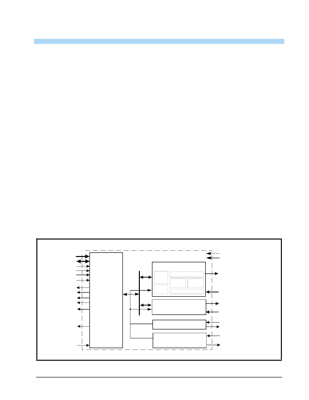
FIGURE 1. XR16C2852 BLOCK DIAGRAM
A 2 :A 0
D 7 :D 0
IO R #
IOW #
CS#
CHSEL
IN T A
IN T B
TXRDYA#
TXRDYB#
MFA#
(O P 2A #,
BAUDOUTA#, or
RXRDYA#)
MFB#
(O P 2B #,
BAUDOUTB#, or
RXRDYB#)
Reset
8-bit Data
Bus
In te r fa c e
UART Channel A
UART
Regs
BRG
128 Byte TX FIFO
TX & RX
IR
ENDEC
128 Byte RX FIFO
UART Channel B
(same as Channel A)
Crystal Osc/Buffer
M odem Control Logic
3.3V or 5V VCC
GND
TXA (or TXIRA)
RXA (or RXIRA)
TXB (or TXIRB)
RXB (or RXIRB)
XTAL1
XTAL2
CTS#A/B, RI#A/B,
CD#A/B, DSR#A/B
DTR#A/B, RTS#A/B
EXAR Corporation 48720 Kato Road, Fremont CA, 94538 • (510) 668-7000 • FAX (510) 668-7017 • www.exar.com • [email protected]
1 page 
XR16C2852
REV. 2.0.0
3.3V AND 5V DUART WITH 128-BYTE FIFO
áç
NAME
GND
44-PLCC
PIN #
22, 12
TYPE
Pwr Power supply common, ground.
DESCRIPTION
Pin type: I=Input, O=Output, I/O= Input/output, OD=Output Open Drain.
1.0 PRODUCT DESCRIPTION
The XR16C2852 (2852) integrates the functions of 2
enhanced 16C550 Universal Asynchrounous Receiv-
er and Transmitter (UART). Each UART is indepen-
dently controlled having its own set of device configu-
ration registers. The configuration registers set is
16550 UART compatible for control, status and data
transfer. Additionally, each UART channel has 128-
bytes of transmit and receive FIFOs, automatic RTS/
CTS hardware flow control with hysteresis control,
automatic Xon/Xoff and special character software
flow control, programmable transmit and receive
FIFO trigger levels, FIFO level counters, infrared en-
coder and decoder (IrDA ver 1.0), programmable
baud rate generator with a prescaler of divide by 1 or
4, and data rate up to 3.125 Mbps. The XR16C2852
is a 5V and 3.3V device. The 2852 is fabricated with
an advanced CMOS process.
Enhanced Features
The 2852 DUART provides a solution that supports
128 bytes of transmit and receive FIFO memory, in-
stead of 64 bytes provided in the XR16L2752 and 16
bytes in the ST16C2552. The 2852 is designed to
work with high performance data communication sys-
tems, that require fast data processing time. In-
creased performance is realized in the 2852 by the
larger transmit and receive FIFOs, FIFO trigger level
control, FIFO level counters and automatic flow con-
trol mechanism. This allows the external processor to
handle more networking tasks within a given time. For
example, the ST16C2552 with a 16 byte FIFO, un-
loads 16 bytes of receive data in 1.53 ms (This exam-
ple uses a character length of 11 bits, including start/
stop bits at 115.2Kbps). This means the external
CPU will have to service the receive FIFO at 1.53 ms
intervals. However with the 128 byte FIFO in the
2852, the data buffer will not require unloading/load-
ing for 12.2 ms. This increases the service interval
giving the external CPU additional time for other ap-
plications and reducing the overall UART interrupt
servicing time. In addition, the programmable FIFO
level trigger interrupt and automatic hardware/soft-
ware flow control is uniquely provided for maximum
data throughput performance especially when operat-
ing in a multi-channel system. The combination of the
above greatly reduces the CPU’s bandwidth require-
ment, increases performance, and reduces power
consumption.
The 2852 supports a half-duplex output direction con-
trol signaling pin, RTS# A/B, to enable and disable
the external RS-485 transceiver operation. It auto-
matically switches the logic state of the output pin to
the receive state after the last stop-bit of the last char-
acter has been shifted out of the transmitter. After re-
ceiving, the logic state of the output pin switches back
to the transmit state when a data byte is loaded in the
transmitter. The auto RS-485 direction control pin is
not activated after reset. To activate the direction con-
trol function, user has to set FCTR Bit-3 to “1”. This
pin is normally high for receive state, low for transmit
state.
Data Rate
The 2852 is capable of operation up to 3.125Mbps at
5V with 16x internal sampling clock rate. The device
can operate with an external 24 MHz crystal on pins
XTAL1 and XTAL2, or external clock source of up to
50MHz on XTAL1 pin. With a typical crystal of
14.7464 MHz and through a software option, the user
can set the prescaler bit for data rates of up to
921.6Kbps.
The rich feature set of the 2852 is available through
the internal registers. Automatic hardware/software
flow control, selectable transmit and receive FIFO
trigger levels, selectable TX and RX baud rates, infra-
red encoder/decoder interface, modem interface con-
trols, and a sleep mode are all standard features.
Following a power on reset or an external reset, the
2852 is software compatible with previous generation
of UARTs, 16C2552 and 16L2752.
5
5 Page 
XR16C2852
REV. 2.0.0
3.3V AND 5V DUART WITH 128-BYTE FIFO
FIGURE 7. TRANSMITTER OPERATION IN NON-FIFO MODE
Data
Byte
Transmit
Holding
Register
(THR)
THR Interrupt (ISR bit-1)
Enabled by IER bit-1
áç
16X
Clock
Transmit Shift Register (TSR)
ML
SS
BB
TXNOFIFO1
2.11.3 Transmitter Operation in FIFO Mode
The host may fill the transmit FIFO with up to 128
bytes of transmit data. The THR empty flag (LSR bit-
5) is set whenever the FIFO is empty. The THR empty
flag can generate a transmit empty interrupt (ISR bit-
1) when the amount of data in the FIFO falls below its
programmed trigger level. The transmit empty inter-
rupt is enabled by IER bit-1. The TSR flag (LSR bit-6)
is set when TSR/FIFO becomes empty.
FIGURE 8. TRANSMITTER OPERATION IN FIFO AND FLOW CONTROL MODE
T rans m it
Data Byte
Auto CTS Flow Control (CTS# pin)
Flow Control Characters
(Xoff1/2 and Xon1/2 Reg.
Auto Software Flow Control
T rans m it
FIFO
THR Interrupt (ISR bit-1) falls
below the programmed Trigger
Level and then when becomes
empty. FIFO is Enabled by FCR
bit-0=1
16X Clock
Transmit Data Shift Register
(TSR)
TXFIFO1
2.12 RECEIVER
The receiver section contains an 8-bit Receive Shift
Register (RSR) and 128 bytes of FIFO which includes
a byte-wide Receive Holding Register (RHR). The
RSR uses the 16X for timing. It verifies and validates
every bit on the incoming character in the middle of
each data bit. On the falling edge of a start or false
start bit, an internal receiver counter starts counting
at the 16X. After 8 clocks the start bit period should
be at the center of the start bit. At this time the start
bit is sampled and if it is still a logic 0 it is validated.
Evaluating the start bit in this manner prevents the re-
ceiver from assembling a false character. The rest of
the data bits and stop bits are sampled and validated
in this same manner to prevent false framing. If there
were any error(s), they are reported in the LSR regis-
ter bits 2-4. Upon unloading the receive data byte
from RHR, the receive FIFO pointer is bumped and
the error tags are immediately updated to reflect the
status of the data byte in RHR register. RHR can gen-
erate a receive data ready interrupt upon receiving a
character or delay until it reaches the FIFO trigger
level. Furthermore, data delivery to the host is guar-
anteed by a receive data ready time-out interrupt
when data is not received for 4 word lengths as de-
fined by LCR[1,0] plus 12 bits time. This is equivalent
to 3.7-4.6 character times. The RHR interrupt is en-
abled by IER bit-0.
11
11 Page | ||
| Páginas | Total 42 Páginas | |
| PDF Descargar | [ Datasheet XR16C2852CJ.PDF ] | |
Hoja de datos destacado
| Número de pieza | Descripción | Fabricantes |
| XR16C2852CJ | 3.3V AND 5V DUART WITH 128-BYTE FIFO | Exar Corporation |
| Número de pieza | Descripción | Fabricantes |
| SLA6805M | High Voltage 3 phase Motor Driver IC. |
Sanken |
| SDC1742 | 12- and 14-Bit Hybrid Synchro / Resolver-to-Digital Converters. |
Analog Devices |
|
DataSheet.es es una pagina web que funciona como un repositorio de manuales o hoja de datos de muchos de los productos más populares, |
| DataSheet.es | 2020 | Privacy Policy | Contacto | Buscar |