|
|
|
PDF ZL10312 Data sheet ( Hoja de datos )
| Número de pieza | ZL10312 | |
| Descripción | Satellite Demodulator | |
| Fabricantes | Zarlink Semiconductor Inc | |
| Logotipo | ||
Hay una vista previa y un enlace de descarga de ZL10312 (archivo pdf) en la parte inferior de esta página. Total 15 Páginas | ||
|
No Preview Available !
ZL10312
Satellite Demodulator
Data Sheet
Features
• Conforms to EBU specification for DVB-S and
DirecTV specification for DSS
• On-chip digital filtering supports 1 - 45 MSps
symbol rates
• On-chip 60 or 90 MHz dual-ADC
• High speed scanning mode for blind symbol
rate/code rate acquisition
• Automatic spectral inversion resolution
• High level software interface for minimum
development time
• Up to ±22 MHz LNB frequency tracking
• DiSEqC™ v2.2: receive/transmit for full control of
LNB, dish and other components
• Compact 64 pin LQFP package (7 x 7 mm)
• Sleep pin gives ~1,000 fold reduction in power to
help products meet ENERGY STAR®
requirements
Applications
• DVB 1 - 45 MSps compliant satellite receiver
• DSS 20 MSps compliant satellite receivers
• SMATV trans-modulators. (Single Master
Antenna TV)
• Satellite PC applications
November 2004
Ordering Information
ZL10312QCG
ZL10312QCF
ZL10312QCG1
ZL10312UBH
64 Pin LQFP Trays, Bake & Drypack
64 Pin LQFP Tape & Reel
64 Pin LQFP* Trays, Bake & Drypack
Die supplied in wafer form**
*Pb Free Matte Tin
**Please contact Sales for further details
0°C to +70°C
Description
The ZL10312 is a QPSK/BPSK 1 - 45 MSps
demodulator and channel decoder for digital satellite
television transmissions to the European Broadcast
Union ETS 300 421 specification. It receives analogue
I and Q signals from the tuner, digitises and digitally
demodulates this signal, and implements the complete
DVB/DSS FEC (Forward Error Correction), and de-
scrambling function. The output is in the form of
MPEG2 or DSS transport stream data packets. The
ZL10312 also provides automatic gain control to the RF
front-end device.
The ZL10312 has a serial 2-wire bus interface to the
control microprocessor. Minimal software is required to
control the ZL10312 because of the built in automatic
search and decode control functions.
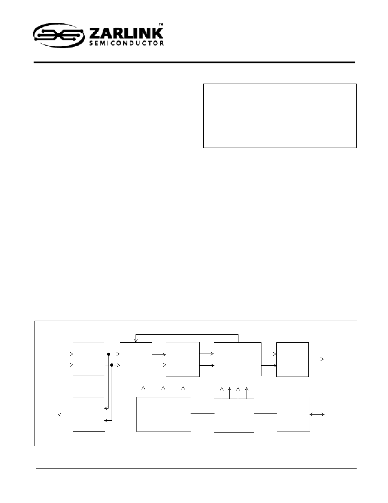
I I/P
Q I/P
Dual ADC
De-rotator
Decimation
Filtering
Timing recovery
Matched filter
Phase recovery
DVB
DSS
FEC
MPEG/
DSS
Packets
Analog
AGC
Control
Clock Generation
Acquisition
Control
2-Wire Bus Bus I/O
Interface
Figure 1 - Functional Block Diagram
1
Zarlink Semiconductor Inc.
Zarlink, ZL and the Zarlink Semiconductor logo are trademarks of Zarlink Semiconductor Inc.
Copyright 2003-2004, Zarlink Semiconductor Inc. All Rights Reserved.
1 page 
ZL10312
Data Sheet
Figure 3 - Typical Application Schematic
5
Zarlink Semiconductor Inc.
5 Page 
ZL10312
Data Sheet
2.6 ZL10312 Pinout Description
Pin Description Table
Pin Name
Description
I/O Note
1 Reset Active low reset input
I CMOS1
2 DiSEqC[2] DiSEqC input for level 2 control. Also usable as I/O Open
GPP2 (general purpose port pin) for other purposes.
drain1
3 DiSEqC[1] Horizontal/vertical LNB control (acts as input only in I/O CMOS
production test modes)
4 DiSEqC[0] 22 kHz output to LNB (acts as input only in I/O CMOS
production test modes)
9
Sleep Stops oscillator and sets minimum power levels to
I CMOS
entire device (except ADCs - register controlled
power-down)
10 CLK1 Primary 2-wire serial bus clock
I CMOS1
11 DATA1 Primary 2-wire serial bus data
I/O Open
drain1
14 DATA2 Secondary 2-wire bus data to tuner front end. Also I/O Open
usable as GPP1 (general purpose port pin) for other
drain1
purposes.
15 CLK2 Secondary 2-wire bus clock to tuner front end. Also I/O Open
usable as GPP0 (general purpose port pin) for other
drain1
purposes.
16 OscMode Controls oscillator mode to suit crystal or external
signal
I CMOS
19 XTI Crystal input or external reference clock input
I CMOS
20
XTO
Crystal output, includes internal feedback resistor to I/O CMOS
XTI
24 Iin I channel input
I analog
25 Iin I channel negative input
I analog
29 Qin Q channel negative input
I analog
30 Qin Q channel input
I analog
35,36,37 ADDR[1:4] Primary 2-wire bus address defining pins
38
I CMOS
41 AGC AGC sigma-delta output (acts as input only in
production test modes)
I/O Open
drain1
V mA
5
56
3.3 2
3.3 2
3.3
5
56
56
56
3.3
1.8
1.8
3.3
56
42
Test For normal operation, this pin must be held at 0V.
I CMOS 3.3
43 IRQ Active low interrupt output. Reading all active
I/O Open
56
interrupt registers resets this pin (acts as input only in
drain1
production test modes)
46 MOSTRT MPEG output start signal. High during the first byte of O CMOS 3.3 2
a packet.
Tri-state
11
Zarlink Semiconductor Inc.
11 Page | ||
| Páginas | Total 15 Páginas | |
| PDF Descargar | [ Datasheet ZL10312.PDF ] | |
Hoja de datos destacado
| Número de pieza | Descripción | Fabricantes |
| ZL10310 | Digital Television DVB-T-On-a-Chip Processor | Zarlink Semiconductor Inc |
| ZL10311 | Digital Television DVB-T-On-a-Chip Processor | Zarlink Semiconductor Inc |
| ZL10311 | Digital Television DVB-T-On-a-Chip Processor | Zarlink Semiconductor Inc |
| ZL10312 | Satellite Demodulator | Zarlink Semiconductor Inc |
| Número de pieza | Descripción | Fabricantes |
| SLA6805M | High Voltage 3 phase Motor Driver IC. |
Sanken |
| SDC1742 | 12- and 14-Bit Hybrid Synchro / Resolver-to-Digital Converters. |
Analog Devices |
|
DataSheet.es es una pagina web que funciona como un repositorio de manuales o hoja de datos de muchos de los productos más populares, |
| DataSheet.es | 2020 | Privacy Policy | Contacto | Buscar |