|
|
|
PDF X88C75 Data sheet ( Hoja de datos )
| Número de pieza | X88C75 | |
| Descripción | Port Expander and E2 Memory | |
| Fabricantes | Xicor | |
| Logotipo | ||
Hay una vista previa y un enlace de descarga de X88C75 (archivo pdf) en la parte inferior de esta página. Total 27 Páginas | ||
|
No Preview Available !
APPLICATION NOTES
AVA I L A B L E
X88C75ASN6L2 •ICAN®64E• A2N66
SLIC X88C75 SLIC® E2 Microperipheral
Port Expander and E2 Memory
FEATURES
• Highly Integrated Microcontroller Peripheral
—8K x 8 E2 Memory
—2 x 8 General Purpose Bidirectional I/O Ports
—16 x 8 General Purpose Registers
—Integerated Interrupt Controller Module
—Internal Programmable Address Decoding
• Self Loading Integrated Code (SLIC)
—On-Chip BIOS and Boot Loader
—IBM/PC Based Interface Software(XSLIC)
• Concurrent Read During Write
—Dual Plane Architecture
• Isolates Read/Write Functions Between Planes
• Allows Continuous Execution Of Code From
One Plane While Writing In The Other Plane
• Multiplexed Address/Data Bus
—Direct Interface to Popular 80C51 Family of
Microcontrollers
• Software Data Protection
—Protect Entire Array During Power-up/-down
• Block Lock™ Data Protection
—Set Write Lockout in 1K Blocks
• Toggle Bit Polling
• High Performance CMOS
—Fast Access Time, 120ns
—Low Power
• 60mA Active
• 100µA Standby
• PDIP, PLCC, and TQFP Packaging Available
DESCRIPTION
The X88C75 SLIC is a highly integrated peripheral for
the 80C51 family of microcontrollers. The device inte-
grates 8K-bytes of 5V byte-alterable nonvolatile memory,
two bidirectional 8-bit ports, 16 general purpose regis-
ters, programmable internal address decoding and a
multiplexed address and data bus.
The 5V byte-alterable nonvolatile memory can be used
as program storage, data storage, or a combination of
both. The memory array is separated into two 4K-bytes
sections which allows read accesses to one section
while a write operation is taking place in the other
section. The nonvolatile memory also features Software
Data Protection to protect the contents during power
transitions, and an advanced Block Protect register
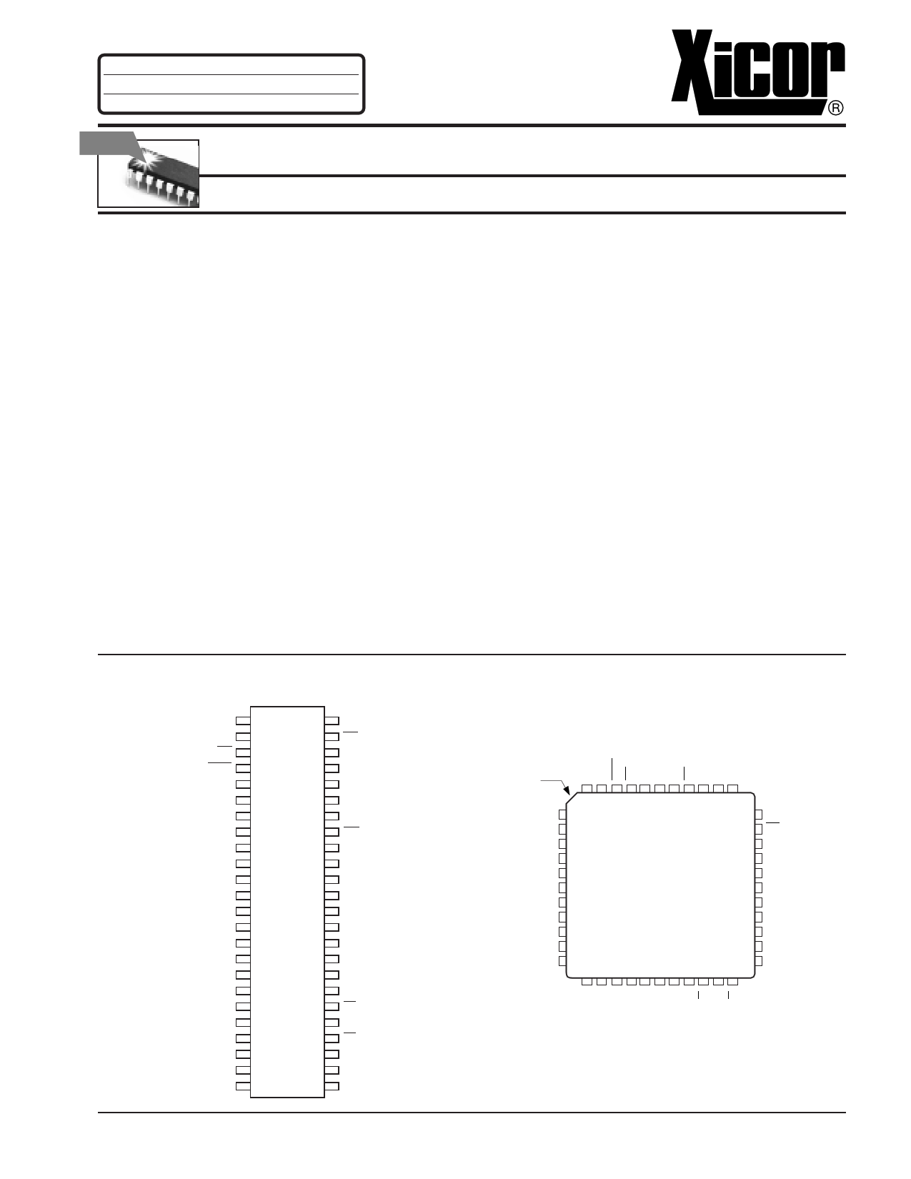
PIN CONFIGURATIONS
DIP
RESET
A12
WC
PSEN
STRA
A15
NC
A14
A13
PA7
PA6
PA5
PA4
PA3
PA2
PA1
PA0
NC
A/D0
A/D1
A/D2
A/D3
A/D4
VSS
1 48
2 47
3 46
4 45
5 44
6 43
7 42
8 41
9 40
10 39
11 38
X88C75
12 37
13 36
14 35
15 34
16 33
17 32
18 31
19 30
20 29
21 28
22 27
23 26
24 25
©Xicor, Inc. 1994, 1995, 1996 Patents Pending
2887-2.5 4/11/97 T0/C0/D1 SH
VCC
WR
ALE
A8
A9
A11
NC
IRQ
STRB
PB7
PB6
PB5
PB4
PB3
PB2
PB1
PB0
NC
RD
A10
CE
A/D7
A/D6
A/D5
28288787ILILLLF0F101
PLCC
TQFP
INDEX
CORNER
A14
A13
PA7
PA6
PA5
PA44
PA3
33
PA2
PA1
PA0
A/D0
6 5 4 3 2 1 44 43 42 41 40
7 39
8 38
9 37
10 36
11 X88C75 35
12 SLIC 34
13 33
14 32
15 31
16 30
17 29
18 19 20 21 22 23 24 25 26 27 28
A11
IRQ
STRB
PB7
PB6
PB5
PB4
PB3
PB2
PB1
PB0
2887 ILL F02.4
Concurrent Read During Write, Block Lock, and
SLIC® E2 are registered trademarks of Xicor, Inc.
1 Characteristics subject to change without notice
1 page 
X88C75 SLIC® E2
DATA PROTECTION
The X88C75 provides two levels of data protection
through software control. There is a global software data
protection feature similar to the industry standard for
E2PROMs and a new Block Lock Protect write lockout
protection providing a secondary level data security
option.
Software Data Protection
Software Data Protection (SDP) can be employed to
protect the entire array against inadvertent writes during
power-up/power-down operations. The X88C75 is
shipped from the factory with SDP enabled. With SDP
enabled, inadvertent attempts to write to the X88C75 will
be blocked.
The system can still write data, but only when the write
operation (page or byte) is preceded by the three-byte
command sequence. All write operations, both the com-
mand sequence and any data write operations must
conform to the page write timing requirements.
The SDP mode is also enabled anytime one of the
nonvolatile configuration registers are modified. These
include writing to EE map, SFR map, and BPR.
Figure 2. Writing With SDP Enabled
AA b2 b1 b0 P 555
55 b2 b1 b0 P AAA
A0 b2 b1 b0 P 555
Perform Byte or
Page Write Operations
Delay of tWC
Exit Routine
2887 ILL F06
b2
b1
b0
Reference the A15–A13
setting in EEM register
P = Address bit (A12) of the
updated memory plane
Figure 3. Sequence to Deactivate Software Data
Protection
AA b2 b1 b0 P 555
55 b2 b1 b0 P AAA
A0 b2 b1 b0 P 555
AA b2 b1 b0 P 555
80 b2 b1 b0 P AAA
Delay of tWC
Exit Routine
2887 ILL F07
b2
b1
b0
Reference the A15–A13
setting in EEM register
P = Address bit (A12) of the
memory plane not being read.
Block Lock Protect Write Lockout
The X88C75 provides a second level of data security
referred to as Block Lock Protect write lockout (or Block
Protect). This is accessed through an extension of the
SDP command sequence. Block Protect allows the user
to lockout writes to 1K x 8 blocks of memory. Unlike SDP
which prevents inadvertent writes, but still allows easy
system access to writing the memory, Block Protect will
lockout all attempts unless it is specifically disabled by
issuing the deactivation sequence. This feature can be
used to set a higher level of protection in a system where
a portion of the memory is used to store the system
kernel and protect it from the application programs
residing in the other blocks.
Setting write lockout is accomplished by writing a five-
byte command sequence opening access to the Block
Protect Register (BPR). After the fifth byte is written, the
user writes to the BPR, selecting which blocks to protect
or unprotect. All write operations, both the command
sequence and writing the data to the BPR, must conform
to the page write timing requirements. It should be noted
5
5 Page 
X88C75 SLIC® E2
PRINCIPLES OF OPERATION
I/O Port Operation
The expansion ports are accessible to the software
using their assigned memory mapped addresses. Each
port occupies two addresses in the SFR plane, the Port
Data Register and Port Pin Register. These registers
and their location in the 1K-byte register memory space
is shown on page 7.
The ports can be configured as either inputs or outputs,
the DIRA and DIRB bits in the configuration register are
used to select between the modes. The input signal on
the strobe pin, when the corresponding port is config-
ured as an input, is fed to the clock input of the port latch.
These are transparent latches and the trailing edge of
the strobe pulse is used to latch the data present on the
input pins. The strobe signal polarity is configurable
using the STPA and STPB bits in the configuration
register.
Writing to the port data register of an output port will
generate a pulse of fixed duration on its strobe pin. The
data also simultaneously arrives at the port output pins.
The latched data stays there until new data is written to
the port data register. The strobe pulse shape is con-
trolled by the state of the STPA and STPB bits in the
configuration register. A “1” forces the valid transition on
the corresponding strobe pin as active HIGH (
),
and a “0” sets it to active LOW (
).
When an external strobe signal is applied to an input
port, the latching of input data is followed by the setting
of the interrupt flags. The INTA and INTB interrupt flags
are used by ports A and B respectively, and are set along
with the INT interrupt flag at the end of strobe pulse input.
External interrupt (IRQ) is generated if the interrupt
enable flags (ENA and ENB) are set by the software.
The former enables the port A interrupt and the latter
enables the port B interrupt.
The port output drivers can be either CMOS or open-
drain. The wire-OR bits (AWO, BWO) in the configura-
tion register are used to make the selection. When the
bits are “0” the CMOS drivers are enabled. Setting these
bits will enable the open-drain output drivers. Small pull-
up resistors should be used on the pins of open-drain
ports.
Figure 12. Block Diagram of the I/O Ports
STROBE (PORT INPUT)
PORT WRITE
(PORT OUTPUT)
LATCH FOR
I/O PIN
PORT
OUTPUT
INPUT
OUTPUT
PORT READ
(PORT INPUT)
I/O
PIN
INTERNAL DATA BUS
PIN READ
(PORT IN OR OUTPUT)
2887 ILL F16.1
11
11 Page | ||
| Páginas | Total 27 Páginas | |
| PDF Descargar | [ Datasheet X88C75.PDF ] | |
Hoja de datos destacado
| Número de pieza | Descripción | Fabricantes |
| X88C75 | Port Expander and E2 Memory | Xicor |
| Número de pieza | Descripción | Fabricantes |
| SLA6805M | High Voltage 3 phase Motor Driver IC. |
Sanken |
| SDC1742 | 12- and 14-Bit Hybrid Synchro / Resolver-to-Digital Converters. |
Analog Devices |
|
DataSheet.es es una pagina web que funciona como un repositorio de manuales o hoja de datos de muchos de los productos más populares, |
| DataSheet.es | 2020 | Privacy Policy | Contacto | Buscar |