|
|
|
PDF V54C3128164VS Data sheet ( Hoja de datos )
| Número de pieza | V54C3128164VS | |
| Descripción | 128Mbit SDRAM 3.3 VOLT/ TSOP II / SOC PACKAGE 8M X 16/ 16M X 8/ 32M X 4 | |
| Fabricantes | Mosel Vitelic Corp | |
| Logotipo | ||
Hay una vista previa y un enlace de descarga de V54C3128164VS (archivo pdf) en la parte inferior de esta página. Total 30 Páginas | ||
|
No Preview Available !
MOSEL VITELIC
V54C3128(16/80/40)4V(T/S)
128Mbit SDRAM
3.3 VOLT, TSOP II / SOC PACKAGE
8M X 16, 16M X 8, 32M X 4
PRELIMINARY
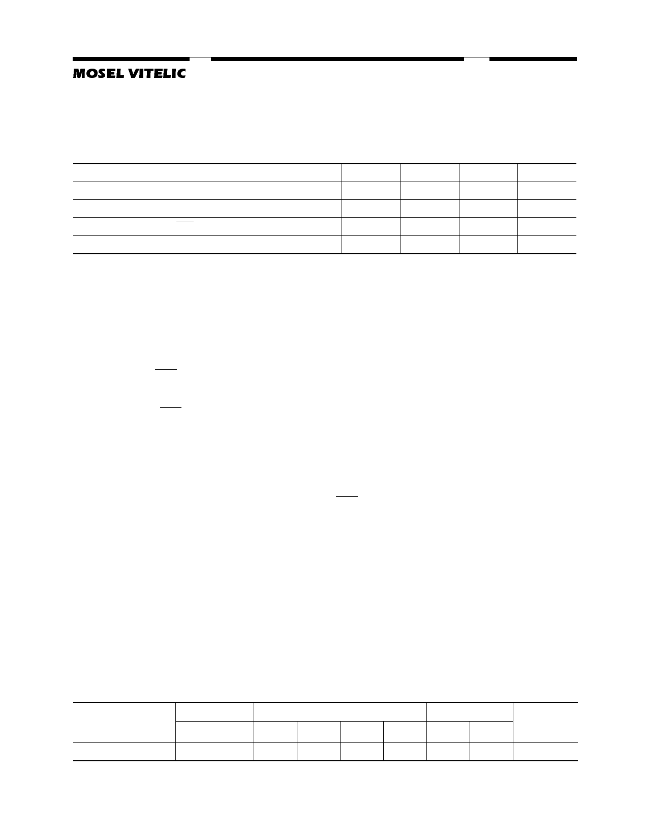
System Frequency (fCK)
Clock Cycle Time (tCK3)
Clock Access Time (tAC3) CAS Latency = 3
Clock Access Time (tAC2) CAS Latency = 2
6
166 MHz
6 ns
5.4 ns
5.4 ns
7PC
143 MHz
7 ns
5.4 ns
5.4 ns
7
143 MHz
7 ns
5.4 ns
6 ns
8PC
125 MHz
8 ns
6 ns
6 ns
Features
■ 4 banks x 2Mbit x 16 organization
■ 4 banks x 4Mbit x 8 organization
■ 4 banks x 8Mbit x 4 organization
■ High speed data transfer rates up to 166 MHz
■ Full Synchronous Dynamic RAM, with all signals
referenced to clock rising edge
■ Single Pulsed RAS Interface
■ Data Mask for Read/Write Control
■ Four Banks controlled by BA0 & BA1
■ Programmable CAS Latency: 2, 3
■ Programmable Wrap Sequence: Sequential or
Interleave
■ Programmable Burst Length:
1, 2, 4, 8 for Sequential Type
1, 2, 4, 8 for Interleave Type
■ Multiple Burst Read with Single Write Operation
■ Automatic and Controlled Precharge Command
■ Random Column Address every CLK (1-N Rule)
■ Power Down Mode
■ Auto Refresh and Self Refresh
■ Refresh Interval: 4096 cycles/64 ms
■ Available in 60-ball SOC BGA and 54 Pin
TSOPII
■ LVTTL Interface
■ Single +3.3 V ±0.3 V Power Supply
Description
The V54C3128(16/80/40)4V(T/S) is a four bank
Synchronous DRAM organized as 4 banks x 2Mbit
x 16, 4 banks x 4Mbit x 8, or 4 banks x 8Mbit x 4.
The V54C3128(16/80/40)4V(T/S) achieves high
speed data transfer rates up to 166 MHz by employ-
ing a chip architecture that prefetches multiple bits
and then synchronizes the output data to a system
clock
All of the control, address, data input and output
circuits are synchronized with the positive edge of
an externally supplied clock.
Operating the four memory banks in an inter-
leaved fashion allows random access operation to
occur at higher rate than is possible with standard
DRAMs. A sequential and gapless data rate of up to
166 MHz is possible depending on burst length,
CAS latency and speed grade of the device.
Device Usage Chart
Operating
Temperature
Range
0°C to 70°C
Package Outline
T/S
•
6
•
Access Time (ns)
7PC 7
••
8PC
•
Power
Std. L
••
Temperature
Mark
Blank
V54C3128(16/80/40)4V(T/S) Rev. 1.2 August 2002
1
1 page 
MOSEL VITELIC
V54C3128(16/80/40)4V(T/S)
Description Pkg.
TSOP-II
T
Pin Count
54
V 54 C 3 12840 4 V A L T
Mosel Vitelic
Manufactured
SYNCHRONOUS
DRAM FAMILY
Device
Number
C=CMOS Family
3.3V, LVTTL INTERFACE
32Mx4(4K Refresh)
4 Banks
Special
Feature
Speed
6 ns
7 ns
8 ns
Component
Package
L=Low Power
Component Rev Level
V=LVTTL
54 Pin Plastic TSOP-II
PIN CONFIGURATION
Top View
VCC
NC
VCCQ
NC
I/O1
VSSQ
NC
NC
VCCQ
NC
I/O2
VSSQ
NC
VCC
NC
WE
CAS
RAS
CS
BA0
BA1
A10
A0
A1
A2
A3
VCC
1
2
3
4
5
6
7
8
9
10
11
12
13
14
15
16
17
18
19
20
21
22
23
24
25
26
27
54 VSS
53 NC
52 VSSQ
51 NC
50 I/O4
49 VCCQ
48 NC
47 NC
46 VSSQ
45 NC
44 I/O3
43 VCCQ
42 NC
41 VSS
40 NC
39 DQM
38 CLK
37 CKE
36 NC
35 A11
34 A9
33 A8
32 A7
31 A6
30 A5
29 A4
28 VSS
Pin Names
CLK
CKE
CS
RAS
CAS
WE
A0–A11
BA0, BA1
I/O1–I/O4
DQM
VCC
VSS
VCCQ
VSSQ
NC
Clock Input
Clock Enable
Chip Select
Row Address Strobe
Column Address Strobe
Write Enable
Address Inputs
Bank Select
Data Input/Output
Data Mask
Power (+3.3V)
Ground
Power for I/O’s (+3.3V)
Ground for I/O’s
Not connected
V54C3128(16/80/40)4V(T/S) Rev. 1.2 August 2002
5
5 Page 
MOSEL VITELIC
Power On and Initialization
The default power on state of the mode register is
supplier specific and may be undefined. The
following power on and initialization sequence
guarantees the device is preconditioned to each
users specific needs. Like a conventional DRAM,
the Synchronous DRAM must be powered up and
initialized in a predefined manner. During power on,
all VCC and VCCQ pins must be built up
simultaneously to the specified voltage when the
input signals are held in the “NOP” state. The power
on voltage must not exceed VCC+0.3V on any of
the input pins or VCC supplies. The CLK signal
must be started at the same time. After power on,
an initial pause of 200 µs is required followed by a
precharge of both banks using the precharge
command. To prevent data contention on the DQ
bus during power on, it is required that the DQM and
CKE pins be held high during the initial pause
period. Once all banks have been precharged, the
Mode Register Set Command must be issued to
initialize the Mode Register. A minimum of eight
Auto Refresh cycles (CBR) are also required.These
may be done before or after programming the Mode
Register. Failure to follow these steps may lead to
unpredictable start-up modes.
Programming the Mode Register
The Mode register designates the operation
mode at the read or write cycle. This register is di-
vided into 4 fields. A Burst Length Field to set the
length of the burst, an Addressing Selection bit to
program the column access sequence in a burst cy-
cle (interleaved or sequential), a CAS Latency Field
to set the access time at clock cycle and a Opera-
tion mode field to differentiate between normal op-
eration (Burst read and burst Write) and a special
Burst Read and Single Write mode. The mode set
V54C3128(16/80/40)4V(T/S)
operation must be done before any activate com-
mand after the initial power up. Any content of the
mode register can be altered by re-executing the
mode set command. All banks must be in pre-
charged state and CKE must be high at least one
clock before the mode set operation. After the mode
register is set, a Standby or NOP command is re-
quired. Low signals of RAS, CAS, and WE at the
positive edge of the clock activate the mode set op-
eration. Address input data at this timing defines pa-
rameters to be set as shown in the previous table.
Read and Write Operation
When RAS is low and both CAS and WE are high
at the positive edge of the clock, a RAS cycle starts.
According to address data, a word line of the select-
ed bank is activated and all of sense amplifiers as-
sociated to the wordline are set. A CAS cycle is
triggered by setting RAS high and CAS low at a
clock timing after a necessary delay, tRCD, from the
RAS timing. WE is used to define either a read
(WE = H) or a write (WE = L) at this stage.
SDRAM provides a wide variety of fast access
modes. In a single CAS cycle, serial data read or
write operations are allowed at up to a 125 MHz
data rate. The numbers of serial data bits are the
burst length programmed at the mode set operation,
i.e., one of 1, 2, 4, 8. Column addresses are seg-
mented by the burst length and serial data accesses
are done within this boundary. The first column ad-
dress to be accessed is supplied at the CAS timing
and the subsequent addresses are generated auto-
matically by the programmed burst length and its
sequence. For example, in a burst length of 8 with
interleave sequence, if the first address is ‘2’, then
the rest of the burst sequence is 3, 0, 1, 6, 7, 4, and
5.
V54C3128(16/80/40)4V(T/S) Rev. 1.2 August 2002
11
11 Page | ||
| Páginas | Total 30 Páginas | |
| PDF Descargar | [ Datasheet V54C3128164VS.PDF ] | |
Hoja de datos destacado
| Número de pieza | Descripción | Fabricantes |
| V54C3128164VAT | High Performance SDRAM | Mosel Vitelic |
| V54C3128164VBGA | 128Mbit SDRAM 3.3 VOLT/ BGA PACKAGE | Mosel Vitelic Corp |
| V54C3128164VS | 128Mbit SDRAM 3.3 VOLT/ TSOP II / SOC PACKAGE 8M X 16/ 16M X 8/ 32M X 4 | Mosel Vitelic Corp |
| V54C3128164VT | 128Mbit SDRAM 3.3 VOLT/ TSOP II / SOC PACKAGE 8M X 16/ 16M X 8/ 32M X 4 | Mosel Vitelic Corp |
| Número de pieza | Descripción | Fabricantes |
| SLA6805M | High Voltage 3 phase Motor Driver IC. |
Sanken |
| SDC1742 | 12- and 14-Bit Hybrid Synchro / Resolver-to-Digital Converters. |
Analog Devices |
|
DataSheet.es es una pagina web que funciona como un repositorio de manuales o hoja de datos de muchos de los productos más populares, |
| DataSheet.es | 2020 | Privacy Policy | Contacto | Buscar |