|
|
|
PDF VECANA01 Data sheet ( Hoja de datos )
| Número de pieza | VECANA01 | |
| Descripción | 10-Channel/ 12-Bit DATA ACQUISITION SYSTEM | |
| Fabricantes | Burr-Brown Corporation | |
| Logotipo | ||
Hay una vista previa y un enlace de descarga de VECANA01 (archivo pdf) en la parte inferior de esta página. Total 17 Páginas | ||
|
No Preview Available !
www.ti.com
VECANA01
VECANA01
10-Channel, 12-Bit
DATA ACQUISITION SYSTEM
FEATURES
q 10 FULLY DIFFERENTIAL INPUTS
q 5 SIMULTANEOUS SAMPLED CHANNELS
PLUS 2 SYNCHRONIZED SAMPLING
CHANNELS
q 3 SYNCHRONIZED 12-BIT ADCs
APPLICATIONS
q AC MOTOR SPEED CONTROLS
q THREE PHASE POWER CONTROL
q UNINTERRUPTABLE POWER SUPPLIES
q VIBRATION ANALYSIS
q 12.8µs THROUGHPUT RATE
q DIGITALLY SELECTABLE INPUT RANGES
q ±5V POWER SUPPLIES
q SERIAL DIGITAL INPUT/OUTPUTS
q 7 SIGN AND 3 DIGITALLY
PROGRAMMABLE WINDOW COMPARATOR
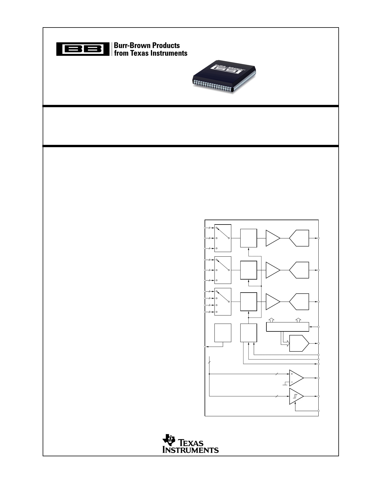
DESCRIPTION
The VECANA01 consists of three 12-bit analog-to-
digital converters preceded by five simultaneously
operating sample-hold amplifiers, and multiplexers
for 10 differential inputs. The ADCs have simulta-
neous serial outputs for high speed data transfer and
data processing.
IUP/N
A1P/N
A2P/N
2
2
2
IVP/N
B1P/N
B2P/N
2
2
2
IWP/N
AN1P/N
AN2P/N
AN3P/N
2
2
2
2
MUX1
MUX2
MUX3
The VECANA01 also offers a programmable gain am-
plifier with programmable gains of 1.0V/V, 1.25V/V,
2.5V
Ref
2.5V/V, and 5.0V/V. Channel selection and gain selec-
REFOUT
tion are selectable through the serial input control word.
The high through put rate is maintained by simulta-
neously clocking in the 13-bit input control word for the
7
next conversion while the present conversions are
clocked out.
SH1 PGA1
ADC1
12-Bit
ADOUT1
SH2 PGA2
ADC2
12-Bit
ADOUT2
SH3 PGA3
ADC3
12-Bit
Control
Logic
Input Select
Gain Select
Input Setup
Register
DAC
DAC
8-Bit
7
ADOUT3
ADIN
DAOUT
ADCLK
ADCONV
ADBUSY
COMP
The part also contains an 8-bit digital-to-analog con-
verter whose digital input is supplied as part of the
input control word.
3 ILIM
DAIN
Copyright © 2000, Texas Instruments Incorporated
SBAS155
Printed in U.S.A. October, 2000
1 page 
PIN DEFINITIONS
PIN NO
1
2
3
4
5
6
7
8
9
10
11
12
13
14
NAME
AN3N
AN3P
AN2N
AN2P
AN1N
AN1P
NC
IWN
IWP
NC
IVN
IVP
NC
B1N
TYPE(1)
AI
AI
AI
AI
AI
AI
—
AI
AI
—
AI
AI
—
AI
15 B1P AI
16 NC —
17 B2N AI
18 B2P AI
19 NC —
20 NC —
21 B_2 DO
22 B_1 DO
23 V_ILIM DO
24 V_COMP DO
25 W_ILIM DO
26 W_COMP DO
27 TP1 —
28 TP2 —
29 UDP5V
P
30 DGND P
31 UDN5V
P
32 NC —
33 ADOUT2 DO
34 ADOUT3 DO
35 ADOUT1 DO
DESCRIPTION
Auxiliary analog input channel 3, Negative Side
Auxiliary analog input channel 3, Positive Side
Auxiliary analog input channel 2, Negative Side
Auxiliary analog input channel 2, Positive Side
Auxiliary analog input channel 1, Negative Side
Auxiliary analog input channel 1, Positive Side
No Connection
Analog input of phase W current, Negative Side
Analog input of phase W current, Positive Side
No Connection
Analog input of phase V current, Negative Side
Analog input of phase V current, Positive Side
No Connection
Signal B analog input of position sensor 1,
Negative Side
Signal B analog input of position sensor 1,
Positive Side
No Connection
Signal B analog input of position sensor 2,
Negative Side
Signal B analog input of position sensor 2,
Positive Side
No Connection
No Connection
Sign of signal B position sensor 2 (B2P, B2N). If
the value is positive (B2P > B2N) B_2 is 1, if the
value is negative (B2P < B2N) B_2 is 0.
Sign of signal B position sensor 1 (B1P, B1N). If
the value is positive (B1P > B1N) B_1 is 1, if the
value is negative (B1P < B1N) B_1 is 0.
Over-current output of phase V, active low. If
IVP-IVN is greater then the positive limiting value
or less than the negative limiting value, U_ILIM
becomes 0.
Sign of phase V current signal (IVP, IVN). If the
value is positive (IVP > IVN) V_COMP is 1, if the
value is negative (IVP < IVN) V_COMP is 0.
Over-current output of phase W, active low. If
IWP-IWN is greater then the positive limiting
value or less than the negative limiting value,
U_ILIM becomes 0.
Sign of phase W current signal (IWP, IWN). If
the value is positive (IWP > IWN) W_COMP is 1,
if the value is negative (IWP < IWN) W_COMP
is 0.
Test pin, do not connect to in normal operation.
Test pin, do not connect to in normal operation.
Digital Supply Voltage, +5V
Digital Supply Voltage, Ground
Digital Supply Voltage, –5V
No Connection
Serial output signal of A/D converter 2. Rising
clock edges of ADCLK outputs the bits of the
A/D converter with MSB first.
Serial output signal of A/D converter 3. Rising
clock edges of ADCLK outputs the bits of the
A/D converter with MSB first.
Serial output signal of A/D converter 1. Rising
clock edges of ADCLK outputs the bits of the
A/D converter with MSB first.
PIN NO
36
NAME
ADCLK
TYPE(1)
DI
37 ADCONV DI
38 NPSH DI
39 ADIN DI
40
ADBUSY
DO
41 DATACLK —
42 NC —
43 NC —
44 NC —
45 NC —
46 U_COMP DO
47 U_ILIM DO
48 A_1 DO
49 A_2 DO
50 NC —
51 NC —
52 A2P AI
53 A2N AI
54 NC —
55 A1P AI
56 A1N AI
57 NC —
58 IUP AI
59 IUN AI
60 NC —
61 DAIN AI
62 DAOUT AO
63
REFOUT
AO
64 REFIN AI
65 REFGND
P
66 UN5V
P
67 AGND
P
68 UP5V
P
DESCRIPTION
Clock for the A/D converters. The nominal clock
frequency is 1.25MHz.
Start signal for the A/D converter, active low. The
first rising clock edge of ADCLK, when ADCONV
is 0, starts the conversion.
Sample/hold control for sampling the position
sensor signals. If the value is 1, the signals are
sampled, if it is 0 they are stored.
Serial input signal for programming the D/A
converter for setting the limit value of the current
signals for the input voltage range of the A/D
converters and for the input multiplexer of the
A/D converters.
Conversion is executing, active low
Test pin, do not connect to in normal operation.
No Connection
No Connection
No Connection
No Connection
Sign of phase U current signal (IUP, IUN). If the
value is positive (IUP > IUN) U_COMP is 1, if
the value is negative (IUP < IUN) U_COMP is 0.
Over-current output of phase U, active low. If
IUP-IUN is greater then the positive limiting value
or less than the negative limiting value, U_ILIM
becomes 0.
Sign of signal A position sensor 1 (A1P, A1N). If
the value is positive (A1P > A1N) A_1 is 1, if the
value is negative (A1P < A1N) A_1 is 0.
Sign of signal A position sensor 2 (A2P, A2N). If
the value is positive (A2P > A2N) A_2 is 1, if the
value is negative (A2P < A2N) A_2 is 0.
No Connection
No Connection
Signal A analog input of position sensor 2,
Negative Side
Signal A analog input of position sensor 2,
Positive Side
No Connection
Signal A analog input of position sensor 1,
Positive Side
Signal A analog input of position sensor 1,
Negative Side
No Connection
Analog input of phase U current, Positive Side
Analog input of phase U current, Negative Side
No Connection
Input for setting the over-current value. Normally
connected to DAOUT
Output of the D/A converter for programming the
over-current limit. Output is programmable from
0V to +2.5V.
Output pin of the integrated reference source,
nominal voltage 2.5V.
Input pin for an external reference voltage.
Ground pin of the reference source.
Analog Supply Voltage, –5V
Analog Supply Voltage, Ground
Analog Supply Voltage, +5V
NOTE: (1) AI is Analog Input, AO is Analog Output, DI is Digital Input, DO is Digital Output, P is Power Supply Connection.
VECANA01
SBAS155
5
5 Page 
INPUT/OUTPUT
The VECANA01 is designed for bipolar input voltages and
uses a binary two’s complement digital output code. A
programmable gain function is associated with each A/D
converter. This changes the full-scale analog input range and
the analog resolution of the converter. Details are shown in
Table IX.
DIFFERENTIAL AND COMMON-MODE INPUT
VOLTAGES
The VECANA01 is designed with full differential signal
paths all the way from the multiplexer inputs through to the
input of the A/D converters. This was done to provide
superior high frequency noise rejection. As is common with
most differential input semiconductor devices, there are
compound restrictions on the combination of differential
and common-mode input voltages. This matter is made
slightly more complicated by the fact that most of the analog
inputs are capable of being affected by the programmable
gain function. The possible differential and single-ended
configurations are shown in Figures 4a and 4b. The maxi-
mum differential and common-mode restrictions are shown
in Table III.
GAIN SELECT CODE
0
1
23
Gain
Full Scale Range
(VD with VCM = 0)
Largest Positive
Common Mode
Voltage, VCM+
Largest Negative
Common Mode
Voltage, VCM–
5.0V/V
±0.5V
2.5V/V
±1.0V
1.25V/V
±2.0V
1.0V/V
±2.5V
+2.7V
+2.4V
+1.9V
+1.6V
–2.7V
–2.4V
–1.9V
–1.6V
TABLE III. Differential and Common Mode Voltage
Restrictions.
(A)
+
VD
2
–
+
VD
2
–
VCM
+–
(B)
+
VD
–
+
VCM
–
IUP
IUP
VD
2
IUN
VD
IUN 2
IU
IUP
VD
IUN
VCM
VCM
VCM
FIGURE 4. (a) Differential Signal Source. (b) Single-ended
Input.
VECANA01
SBAS155
INPUT SETUP
As the A/D converters are converting and transmitting their
serial digital data for one conversion cycle, a setup word is
received to be used for the next conversion cycle. The 13-bit
word is supplied at the ADIN pin (see Figure 1), and is
stored in the buffered Input Setup Register. The Input Select
and Gain Select portions of the word are decoded and
determine the state of the multiplexers and PGAs (see
CONFIGURABLE PARAMETERS section).
INPUT MULTIPLEXER AND SAMPLE HOLD
SELECTION
The Input Select portion of the ADIN word (bits 10, 11 and
12) (see Figure 2) are decoded and determine the open/
closed condition of the multiplexer switches. This in turn
determines which input signals are connected to the sample
and holds and which sample and holds are connected to the
PGAs/ADCs.
SIGN OF THE INPUT SIGNALS
The VECANA01 contains seven comparators, which ac-
quire the signals of the first seven input analog signals. The
digital outputs of the sign comparators are the signals
X_COMP. If the positive input value is greater than the
negative input value, the X-COMP output becomes High
(logic “1”) or if the reverse, the X-COMP output is Low
(logic “0”), (see Table IV).
IUP – IUN
A1P – A1N
A2P – A2P
IVP – IVN
B1P – B1N
B2P – B2N
IWP – IWN
>0
<0
TABLE IV. Input - Output Relation.
U_COMP
A_1
A_2
V_COMP
B_1
B_2
W_COMP
1
0
The typical hysteresis value of comparators U_COMP,
V_COMP and W_COMP is 10mV. The typical hysteresis
value of comparators A_1, A_2, B_1, and B_2 is 50mV. AC
motor control applications will typically use 10mV hysteresis
for phase current measurement and 50mV hysteresis for
positioning sensor measurement.
OVER RANGE RECOGNITION
The VECANA01 also includes three window comparators for
the three input signals IU, IV and IW. Each window compara-
tor is composed of two comparators that are monitoring the
input value on the positive range limit (UPLIM) and negative
range limit (UNLIM). The output values of the window com-
parators are output via the pins U_ILIM, V_ILIM and
W_ILIM. The two range limiting values are symmetrical to
the zero point (UNLIM = –UPLIM) and are determined by pin
11
11 Page | ||
| Páginas | Total 17 Páginas | |
| PDF Descargar | [ Datasheet VECANA01.PDF ] | |
Hoja de datos destacado
| Número de pieza | Descripción | Fabricantes |
| VECANA01 | 10-Channel/ 12-Bit DATA ACQUISITION SYSTEM | Burr-Brown Corporation |
| VECANA01 | 10-Channel 12-Bit Data Acquisition System | Texas Instruments |
| Número de pieza | Descripción | Fabricantes |
| SLA6805M | High Voltage 3 phase Motor Driver IC. |
Sanken |
| SDC1742 | 12- and 14-Bit Hybrid Synchro / Resolver-to-Digital Converters. |
Analog Devices |
|
DataSheet.es es una pagina web que funciona como un repositorio de manuales o hoja de datos de muchos de los productos más populares, |
| DataSheet.es | 2020 | Privacy Policy | Contacto | Buscar |