|
|
PDF VG3617161BT Data sheet ( Hoja de datos )
| Número de pieza | VG3617161BT | |
| Descripción | 16Mb CMOS Synchronous Dynamic RAM | |
| Fabricantes | ETC | |
| Logotipo |  |
|
Hay una vista previa y un enlace de descarga de VG3617161BT (archivo pdf) en la parte inferior de esta página. Total 30 Páginas | ||
|
No Preview Available !
VIS
VG3617161BT
16Mb CMOS Synchronous Dynamic RAM
Description
The VG3617161BT is CMOS Synchronous Dynamic RAM organized as 524,288-word X 16-bit X 2-bank.
It is fabricated with an advanced submicron CMOS technology and designed to operate from a single 3.3V
power supply. This SDRAM is delicately designed with performance concern for current high-speed applica-
tion. Programmable CAS Latency and Burst Length make it possible to be used in widely various domains. It
is packaged by using JEDEC standard pinouts and standard plastic 50-pin TSOP II.
Features
• Single 3.3V +/- 0.3V power supply
• Clock Frequency: 200MHz, 183MHz, 166MHz, 143MHz, 125MHz
• Fully synchronous with all signals referenced to a positive clock edge
• Programmable CAS Iatency (2,3)
• Programmable burst length (1,2,4,8,& Full page)
• Programmable wrap sequence (Sequential/Interleave)
• Automatic precharge and controlled precharge
• Auto refresh and self refresh modes
• Dual internal banks controlled by A11(Bank select)
• Simultaneous and independent two bank operation
• I/O level : LVTTL interface
• Random column access in every cycle
• X16 organization
• Byte control by LDQM and UDQM
• 2048 refresh cycles/32ms
• Burst termination by burst stop and precharge command
Document:1G5-0150
Rev.4
Page 1
1 page 
VIS
VG3617161BT
16Mb CMOS Synchronous Dynamic RAM
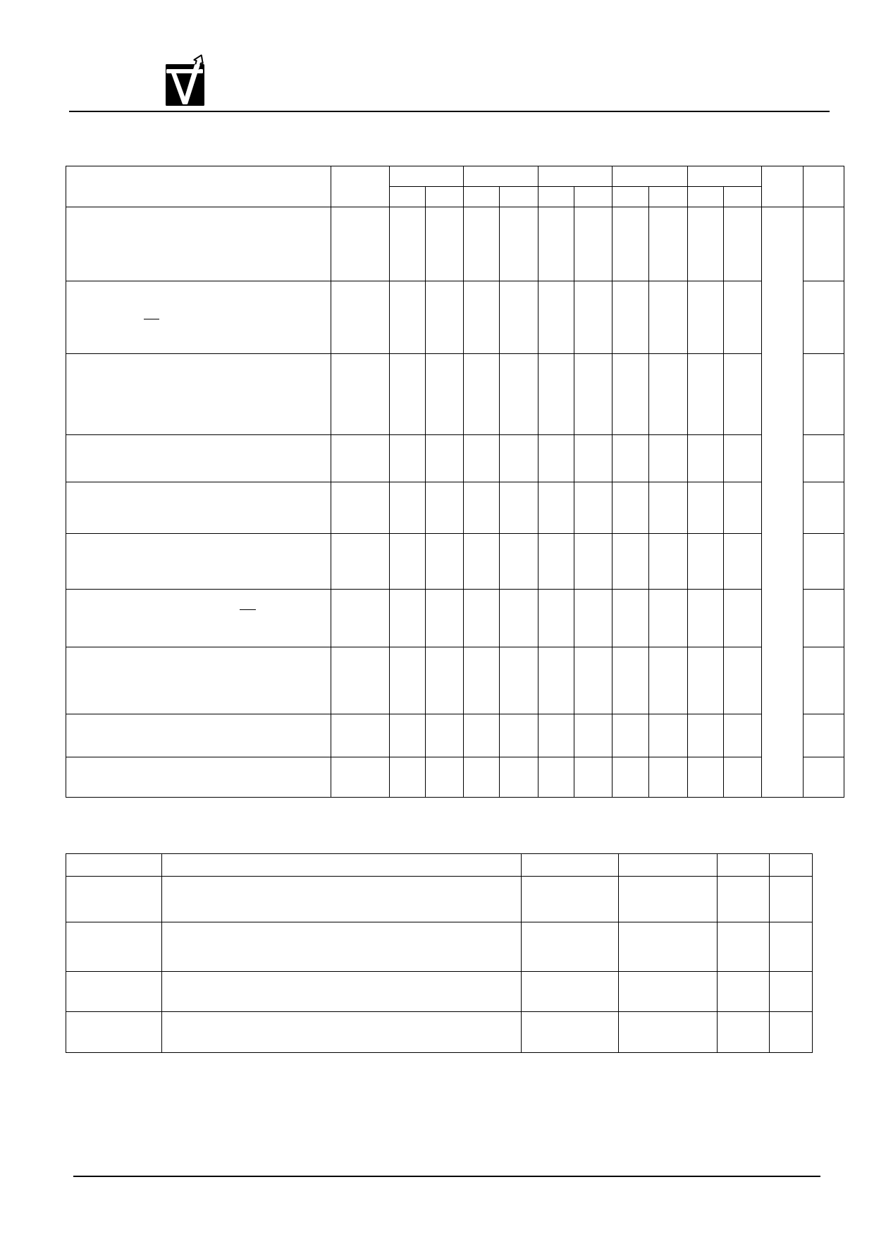
Recommended D.C. Operating Conditions (VDD = 3.3V ± 0.3V, Ta = 0 ~ 70°C)
Description/test condition
-5 -5.5 -6 -7 -8
Symbol Min. Max. Min. Max. Min. Max. Min. Max. Min. Max.
Operating Current
tRC ≥ tRC(min), Outputs Open
Address changed once during tCK(min).
Burst Length = 1 (One Bank Active)
IDD1 195 190 185 165 145
Precharge Standby Current in non power-down
IDD2N
105 95
85
75
65
mode
tCK = tCK(min), CS ≥ VIH(min), CKE ≥ VIH (min)
Input signals are changed once during 30ns.
Precharge Standby Current in non power-down
IDD2NS
50
45
40
35
30
mode
≤tCK = ∞ , CKE ≥ VIH (min), CLK VIL (max)
Input signals are stable
Precharge Standby Current in power-down mode IDD2P 4 4 4 4 4
tCK = tCK(min), CKE ≤ VIL (max)
Unit
mA
Note
3,4
3
3
Precharge Standby Current in power-down mode IDD2PS 3.5 3.5 3.5 3.5 3.5
≤tCK = ∞ , CKE ≤ VIL (max), CLK VIL (max)
Active Standby Current in non power down mode
≥CKE VIH (min), tCK = tCK(min)(Both Bank
Actioe)
Active Standby Current in power-down
≤ ≥CKE VIL (max), tCK = tCK(min), CS
VIH(min)(Both Bank Active)
Operating Current (Page Burst, and All Bank acti-
vated)
tCCD = tCCD(min), Outputs Open, Multi-bank inter-
leave, gapless data
Refresh Current
tRC ≥ tRC (min) (tREF = 32ms)
Self Refresh Current
CKE ≤ 0.2V
IDD3N
IDD3P
IDD4
IDD5
IDD6
90 85 75 65 55
666 66
200 195 185 175 165
190 185 175 165 155
444 44
3
4,5
3
Parameter
IIL
IOL
VOH
VOL
Description
Input Leakage Current
( 0V ≤ VIN ≤ VDD All other pins not under test = OV)
Output Leakage Current
Output disable, (0V ≤ VOUT ≤ VDDQ )
LVTTL Output ”H” Level Voltage
(lOUT = -2mA)
LVTTL Output ”L” Level Voltage
(lOUT = 2mA)
A.C Characteristics:
Test Conditions: (Ta=0 to 70°C VDD=3.3V ±0.3V ,VSS=0V)
Document:1G5-0150
Rev.4
Min.
-5
-5
2.4
-
Max.
5
5
-
0.4
Unit Note
µA
µA
V
V
Page 5
5 Page 
VIS
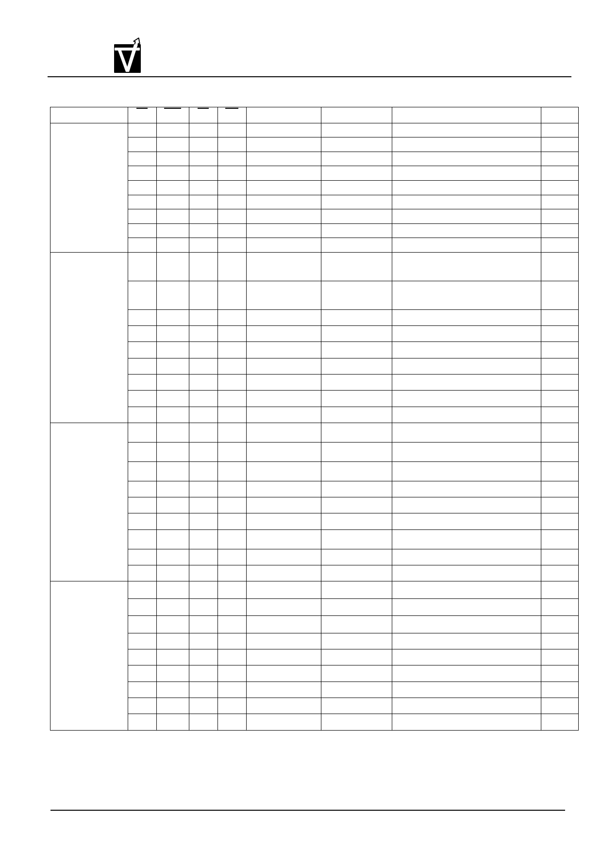
Current state
Read with auto
precharge
Write with auto
precharge
Precharging
Row activating
CS RAS CA WE Address
H X X XX
L H H HX
L H H LX
L H L H BA,CA,A10
L H L L BA,CA,A10
L L H H BA,RA
L L H L BA,A10
L L L HX
L L L L Op-Code
H X X XX
L H H HX
L H H LX
L H L H BA,CA,A10
L H L L BA,CA,A10
L L H H BA,RA
L L H L BA,A10
L L L HX
L L L L Op-code
H X X XX
L H H HX
L H H LX
L H L H BA,CA,A10
L H L L BA,CA,A10
L L H H BA,RA
L L H L BA,A10
L L L HX
L L L L Op-Code
H X X XX
L H H HX
L H H LX
L H L H BA,CA,A10
L H L L BA,CA,A10
L L H H BA,RA
L L H L BA,A10
L L L HX
L L L L Op-Code
VG3617161BT
16Mb CMOS Synchronous Dynamic RAM
Command
DESL
NOP
BST
READ/READA
WRIT/WRITA
ACT
PRE/PALL
PEF/SELF
MRS
DESL
NOP
BST
READ/READA
WRIT/WRITA
ACT
PRE/PALL
REF/SELF
MRS
DESL
NOP
BST
READ/READA
WRIT/WRITA
ACT
PRE/PALL
REF/SELF
MRS
DESL
NOP
BST
READ/READA
WRIT/WRITA
ACT
PRE/PALL
REF/SELF
MRS
(2/3)
Action
Continue burst to end → Prech arging
Continue burst to end → Prech arging
ILLEGAL
ILLEGAL
ILLEGAL
ILLEGAL
ILLEGAL
ILLEGAL
ILLEGAL
Continue burst to end → Write
recovering with auto precharge
Continue burst to end → Write
recovering with auto precharge
ILLEGAL
ILLEGAL
ILLEGAL
ILLEGAL
ILLEGAL
ILLEGAL
ILLEGAL
Nop → Enter idle after tRP
Nop → Enter idle after tRP
Nop → Enter idle after tRP
ILLEGAL
ILLEGAL
ILLEGAL
Nop → Enter idle after tRP
ILLEGAL
ILLEGAL
Nop → Enter row active after tRCD
Nop → Enter row active after tRCD
Nop → Enter row active after tRCD
ILLEGAL
ILLEGAL
ILLEGAL
ILLEGAL
ILLEGAL
ILLEGAL
Notes
3
3
3
3
3
3
3
3
3
3,10
3
Document:1G5-0150
Rev.4
Page 11
11 Page | ||
| Páginas | Total 30 Páginas | |
| PDF Descargar | [ Datasheet VG3617161BT.PDF ] | |
Hoja de datos destacado
| Número de pieza | Descripción | Fabricantes |
| VG3617161BT | 16Mb CMOS Synchronous Dynamic RAM | ETC |
| Número de pieza | Descripción | Fabricantes |
| SLA6805M | High Voltage 3 phase Motor Driver IC. |
Sanken |
| SDC1742 | 12- and 14-Bit Hybrid Synchro / Resolver-to-Digital Converters. |
Analog Devices |
|
DataSheet.es es una pagina web que funciona como un repositorio de manuales o hoja de datos de muchos de los productos más populares, |
| DataSheet.es | 2020 | Privacy Policy | Contacto | Buscar |
