|
|
|
PDF TSM101P Data sheet ( Hoja de datos )
| Número de pieza | TSM101P | |
| Descripción | VOLTAGE AND CURRENT CONTROLLER | |
| Fabricantes | STMicroelectronics | |
| Logotipo | ||
Hay una vista previa y un enlace de descarga de TSM101P (archivo pdf) en la parte inferior de esta página. Total 15 Páginas | ||
|
No Preview Available !
® TSM101/A
VOLTAGE AND CURRENT CONTROLLER
. 1.24V SERIES VOLTAGE REFERENCE WITH
. 10mA OUTPUT CURRENT AND 1% PRECI-
SION (TSM101A)
TWO OPERATIONAL AMPLIFIERS WITH
ORED OUTPUT AND 1MHZ GAIN BAND-
WIDTH PRODUCT
. BUILT-IN CURRENT GENERATOR WITH EN-
ABLE/DISABLE FUNCTION
. 4.5 TO 32V SUPPLY VOLTAGE RANGE
. SO8, DIP8 AND TSSOP8 PACKAGES
N
DIP8
(Plastic Package)
D
SO8
(Plastic Micropackage)
P
TSSO P8
(Thin Shrink Small Outline Package)
DESCRIPTION
The TSM101/TSM101Aintegrated circuit incorpo-
rates a high stability series band gap voltage refer-
ence, two ORed operational amplifiers and a
current source.
This IC compares the DC voltage and the current
level at the output of a switching power supply to
an internal reference. It provides a feedback
through an optocoupler to the PWM controller IC in
the primary side.
The controlled current generator can be used to
modify the level of current limitation by offsetting
the information coming from the current sensing
resistor.
APPLICATIONS
This circuit is designed to be used in battery charg-
ers with a constant voltage and a limited output
current.
It can be used in every types of applicationrequiring
a precision voltage regulation and current limita-
tion.
Other applications include voltage supervisors,
over voltage protection...
June 1999
ORDER CODES
Part Number
TSM101C/AC
TSM101I/AI
Temperature
Range
-20, +80oC
-40, +105oC
Package
NDP
•••
•••
PIN CONNECTIONS
1 Vref 8
27
36
45
1/15
1 page 
TSM101/A
APPLICATION NOTE
A BATTERY CHARGER USING THE TSM101
by S. LAFFONT and R. LIOU
This technical note shows how to use the TSM101
integrated circuit with a switching mode power
supply (SMPS) to realize a battery charger.
An example of realization of a 12V Nickel-cadmium
battery charger is given.
1 - TSM101 PRESENTATION
The TSM101 integrated circuit incorporates a high
stability series band gap voltage reference, two
ORed operational amplifiers and a current source
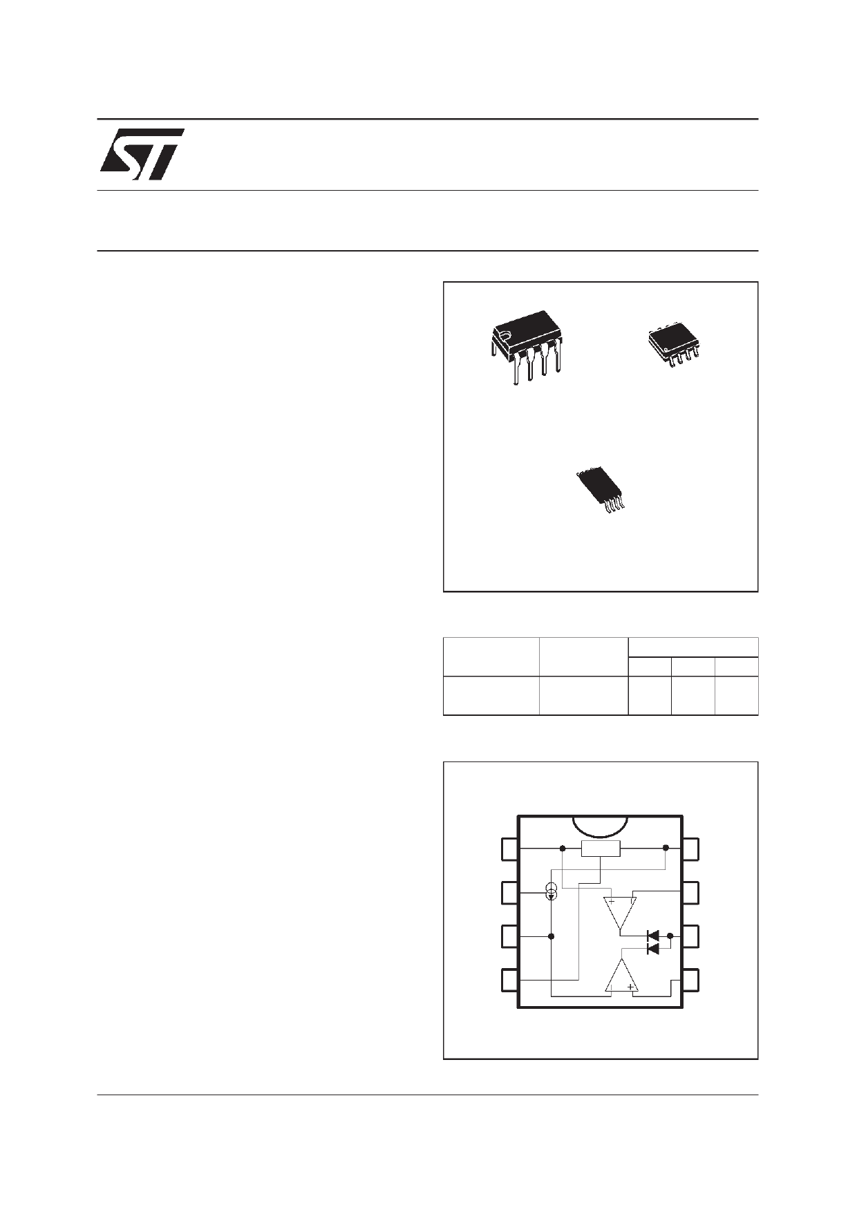
(Figure 1)
Figure 1 : TSM101 Schematic Diagram
1 Vref 8
27
36
45
This IC compares the DC voltage and the current
level at the output of a switching power supply to
an internal reference.It provides a feedback
through an optocoupler to the PWM controller IC in
the primary side.
The controlled current generator can be used to
modify the level of current limitation by offsetting
the information coming from the current sensing
resistor.
A great majority of low or medium end power
supplies is voltage regulated by using shunt pro-
grammable voltage references like the TL431
(Figure 2).
The galvanic insulation of the control information is
done by using an opto-coupler in linear mode with
a variable photo current depending on the differ-
ence between the actual output voltage and the
desired one.
A current limitation is used to protect the power
supply against short circuits, but lacks precision.
This limitation is generally realized by sensing the
current of the power transistor, in the primary side
of the SMPS.
The role of the TSM101 is to make a fine regulation
of the output current of the SMPS and a precise
voltage limitation.
The primary current limitation is conserved and
acts as a security for a fail-safe operation if a
short-circuit occurs at the output of the charger.
2 - PRINCIPLE OF OPERATION
The current regulation loop and the voltage limita-
tion loop use an internal 1.24V band-gap voltage
reference. This voltage reference has a good pre-
cision (better than 1.5%) and exhibits a very stable
temperature behavior.
The current limitation is performed by sensing the
voltage across the low ohmic value resistor R5 and
comparing it to a fixed value set by the bridge
composed by R2 and R3 (Figure 3).
When the voltage on R5 is higher than the voltage
on R3 the output of the current loop operational
amplifier decreases. The optocoupler current in-
creases and tends to reduce the output voltage by
the way of the PWM controller.
The voltage regulation is done by comparing a part
of the output voltage (resistor bridge R6, R7 and
P1) to the voltage reference (1.24V).
If this part is higher than 1.24V, the output of the
voltage loop operational amplifier decreases.
5/15
5 Page 
TSM101/A
EVALUATION BOARD - TECHNICAL NOTE
TSM101 integrates in the same 8 pin DIP or SO
package
• one 1.24V precision voltage reference
• two operationnal amplifiers
• two diodes which impose a NOR function on the
outputs of the operationnal amplifiers
• one current source which can be activated/ inhib-
ited thanks to an external pin.
An immediate way to take advantage of the high
integration and reliability of TSM101 is to use it as
a voltage and current controller on power supplies
secondary. The application note AN896 describes
precisely how to use TSM101 in an SMPS battery
charger.
The TSM101 Evaluation Board is adaptable to any
power supply or battery charger (SMPS or linear)
as a voltage and current controller with minimal
constraints from the user.
HOW TO USE THE TSM101 EVALUATION
BOARD ?
The generic Electrical Schematic is shown on fig-
ure 1. It represents an incomplete SMPS power
supply where the primary side is simplified.
The ”IN+”and ”IN-” power inputs of the evalu-
ation board should be connected directly to the
power lines of the power supply secondary.
The ”Vcc” input of the evaluation board should be
connected to the auxiliary supply line.
In the case of an SMPS power supply, the ”Reg”
output of the evaluation board should be con-
nected to the Optocoupler input to regulate the
PWM block in the primary side. In the case of a
linear power supply, the ”Reg” output should be
connected to the base of the darlington to regulate
the power output.
A diode might be needed on the output of the
evaluation board in the case of a battery charger
application to avoid the discharge of the battery
when the charger is not connected.
COMPONENTS CALCULATIONS
The voltage control is given by the choice of the
resistor bridge R6/R7 (and the trimmer P1) due to
equation 1 :
• Vref = R6/(R6+R7)xVout
where Vref = 1.24V
eq1
Figure 1
11/15
11 Page | ||
| Páginas | Total 15 Páginas | |
| PDF Descargar | [ Datasheet TSM101P.PDF ] | |
Hoja de datos destacado
| Número de pieza | Descripción | Fabricantes |
| TSM101 | VOLTAGE AND CURRENT CONTROLLER | STMicroelectronics |
| TSM101 | VOLTAGE AND CURRENT CONTROLLER | STMicroelectronics |
| TSM1011 | Constant Voltage and Constant Current Controller for Battery Chargers and Adapters | STMicroelectronics |
| TSM1011AID | Constant Voltage and Constant Current Controller for Battery Chargers and Adapters | STMicroelectronics |
| Número de pieza | Descripción | Fabricantes |
| SLA6805M | High Voltage 3 phase Motor Driver IC. |
Sanken |
| SDC1742 | 12- and 14-Bit Hybrid Synchro / Resolver-to-Digital Converters. |
Analog Devices |
|
DataSheet.es es una pagina web que funciona como un repositorio de manuales o hoja de datos de muchos de los productos más populares, |
| DataSheet.es | 2020 | Privacy Policy | Contacto | Buscar |