|
|
|
PDF TK75005DCMG Data sheet ( Hoja de datos )
| Número de pieza | TK75005DCMG | |
| Descripción | LOW-COST FLEXIBLE PWM CONTROLLER | |
| Fabricantes | TOKO | |
| Logotipo | ||
Hay una vista previa y un enlace de descarga de TK75005DCMG (archivo pdf) en la parte inferior de esta página. Total 9 Páginas | ||
|
No Preview Available !
TK75005
ADVANCED
INFORMATION
LOW-COST FLEXIBLE PWM CONTROLLER
FEATURES
s Can Be Used For Power Factor Correction/Line
Harmonics Reduction to Meet IEC1000-3-2
Requirements
s Maximum Duty Ratio 89% (typ.)
s Low Standby Current for Current-Fed Start-Up
s Current-Mode or Voltage-Mode Control
s Internal User-Adjustable Slope Compensation
s Pulse-by-Pulse Current Limiting
APPLICATIONS
s Power Factor Correction Converters
s Off-Line Power Supplies
s Industrial Power Supplies
s Off-Line Battery Charger
TK75005
DESCRIPTION
The TK75005 is an 8-pin PWM controller suitable for both
voltage-mode and current-mode control. It also has
advanced features not available in controllers with a higher
pin count. One such feature is a sawtooth current flowing
out of the feedback pin (FB), which provides a slope
compensation ramp (in current mode applications) in
proportion to the resistance terminating that FB pin.
The TK75005 offers the same features as the TK75003
with the addition of the Error Amplifier and the Overvoltage
Protection (OVP) functions, and the deletion of the
Overcurrent Frequency Reduction feature.
This PWM has features similar to the UC3842 (please
refer to UC3842 Comparison Section).
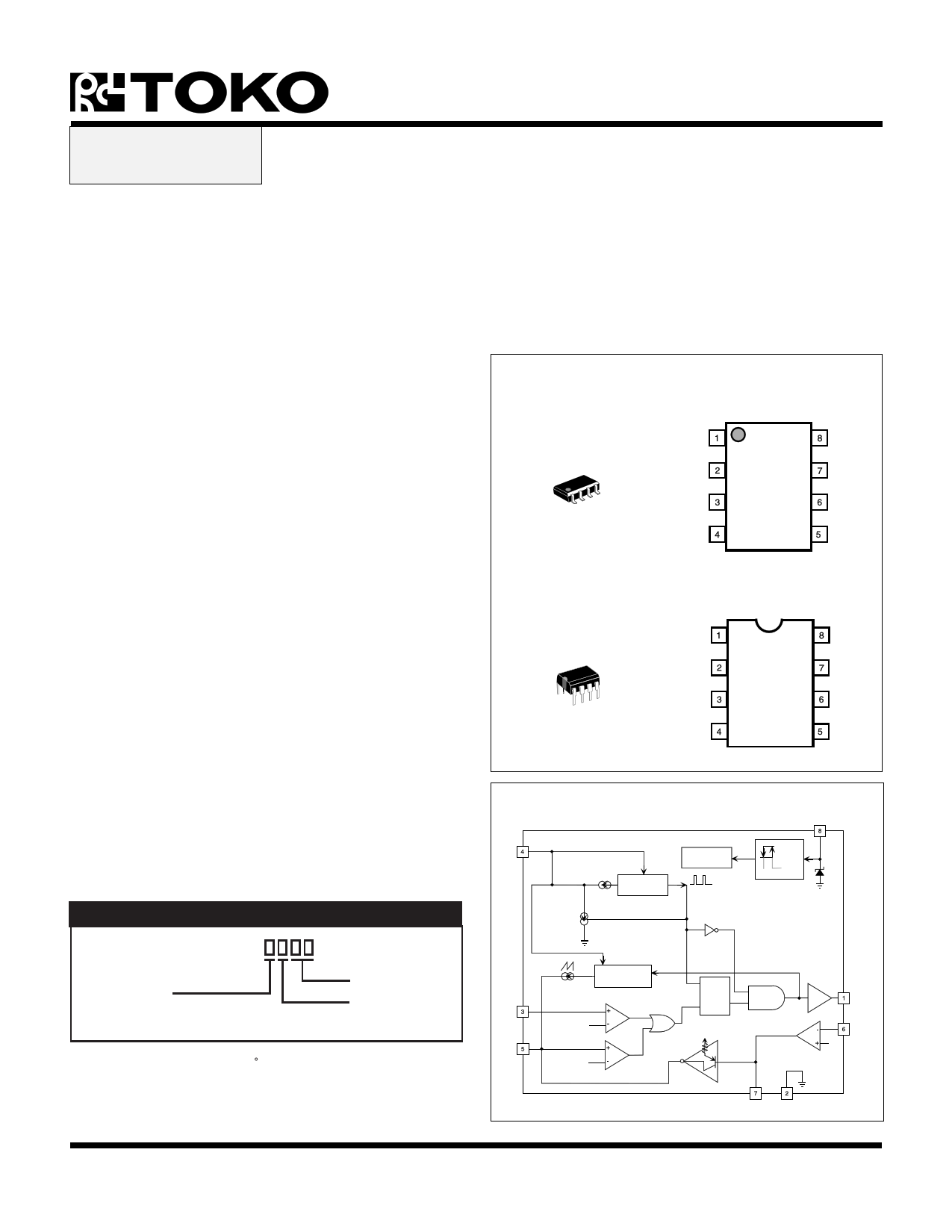
75005
SOP-8
DRV
GND
OVP
CT
75005
DIP-8
DRV
GND
OVP
CT
VCC
EAOUT
EAIN
FB
VCC
EAOUT
EAIN
FB
ORDERING INFORMATION
TK75005
Package Code
Tape/Reel Code
Temp. Range
PACKAGE CODE
D: DIP-8
M: SOP-8
TEMPERATURE RANGE
C: -40 TO 80 C
TAPE/REEL CODE
TL: Tape Left
MG: Magazine
ICT
CT
BLOCK DIAGRAM
VCC
ICHG
175 µA
IDS
1.975 mA
OSCILLATOR
BANDGAP
REFERENCE
fCLK
UVLO
10.0 V
8.0 V
OVP
FB
SLOPE
COMPENSATION
OVERVOLTAGE
DETECTOR
PWM LATCH
SQ
R
2.6 V
CURRENT
CONTROL
DETECTOR
1.02 V
GM STAGE
DRV
EAIN
2.5 V
EAOUT GND
January 1999 TOKO, Inc.
Page 1
1 page 
TK75005
PIN DESCRIPTIONS
DRIVE PIN (DRV)
This pin drives the external MOSFET with a totem pole
output stage capable of sinking or sourcing a peak current
of about 1 A. In standby mode, the DRV pin can sink about
5 mA while keeping the drive pin pulled down to about 1 V.
This ensures that the external MOSFET can not be
inadvertently turned on by leakage currents. The maximum
duty cycle of the output signal is typically 89%.
GROUND PIN (GND)
This pin provides ground return for the IC.
OVERVOLTAGE PROTECTION INPUT PIN (OVP)
This pin provides a means of turning off the external
transistor drive output independent of the PWM loop. This
pin is normally used for overvoltage protection, but can
also be used to provide a drive disabled function. The pin
is the input to comparator with its other input referenced to
2.6 V, which tracks Vref of error amp over temperature. and
its output controlling the output driver of the IC. Therefore,
if a voltage appears at this pin over 2.6 V, the voltage at
the DRV pin drops to zero.
TIMING CAPACITOR PIN (CT)
The external timing capacitor is connected to the CT pin.
That capacitor is the only component needed for setting
the clock frequency. The frequency measured at the CT pin
is the same frequency as measured at the DRV pin. As the
frequency of operation increases above 200 kHz, the
maximum duty cycle decreases from a typical 89% at
200 kHz to 82% at 1.6 MHz. The maximum recommended
clock frequency of the device is 1.6 MHz. At normal
operation, during the rising section of the timing-capacitor
voltage, a trimmed internal current of 175 µA flows out from
the C pin and charges the capacitor. During the falling
T
section of the timing-capacitor voltage, an internal current
of about 1.8 mA discharges the capacitor.
FEEDBACK INPUT PIN (FB)
The feedback pin normally receives the sum of three
signals: the switch current signal, the error signal (from the
internal error amplifier and the GM stage), and a voltage
ramp (from an internal sawtooth-shaped current with a
peak value of about 205 µA) generated across the external
terminating resistance. The switch current signal is needed
in current-mode controlled converters and in converters
with cycle-by-cycle overload protection. The error signal is
needed for stabilizing the output voltage or current. The
voltage ramp is needed for slope compensation (necessary
for avoiding subharmonic instability in constant-frequency
peak-current controlled current-mode converters above
50% duty ratio), or for Pulse Width Modulation (PWM) (in
voltage-mode controlled converters).
At higher clock frequencies, the bandwidth limitation of the
internally-generated sawtooth-shaped current source
becomes more apparent. The degree to which ramp
bandwidth is tolerable depends on performance
requirements at narrow pulse widths. A low impedance at
the feedback pin can effectively eliminate the internally-
generated ramp effects and an external ramp can be
readily created to attain higher performance at high
frequencies, if desired.
ERROR AMPLIFIER COMPENSATION INPUT PIN (EAIN)
This pin is the inverting input of an operational amplifier
which has its non-inverting input connected to 2.5 V. This
is called the error amp because it amplifies the error
between this pin’s voltage and 2.5 V reference, which
should reflect the error in the power supply’s output
regulation. The error amp provides a high gain stage so
that the voltage loop gain can be high enough to provide
good output voltage regulation.
ERROR AMPLIFIER COMPENSATION OUTPUT PIN (EAOUT)
This pin is the output of the operational amplifier mentioned
in the EAIN pin description. By picking the proper resistor
and capacitor network connected between pins 6 and 7,
the gain and frequency response of the error amp block of
the voltage loop can be set, thus providing gain and
frequency compensation into the PWM voltage loop as
needed. This pin also acts as the input to the GM stage of
the voltage control loop.
SUPPLY VOLTAGE PIN (VCC)
This pin is connected to the supply voltage. The IC is in a
low-current (250 µA typ.) standby mode before the supply
voltage exceeds 10 V (typ.), which is the upper threshold
of the undervoltage lockout circuit. The IC switches back
to standby mode when the supply voltage drops below 8 V
(typ.).
January 1999 TOKO, Inc.
Page 5
5 Page | ||
| Páginas | Total 9 Páginas | |
| PDF Descargar | [ Datasheet TK75005DCMG.PDF ] | |
Hoja de datos destacado
| Número de pieza | Descripción | Fabricantes |
| TK75005DCMG | LOW-COST FLEXIBLE PWM CONTROLLER | TOKO |
| Número de pieza | Descripción | Fabricantes |
| SLA6805M | High Voltage 3 phase Motor Driver IC. |
Sanken |
| SDC1742 | 12- and 14-Bit Hybrid Synchro / Resolver-to-Digital Converters. |
Analog Devices |
|
DataSheet.es es una pagina web que funciona como un repositorio de manuales o hoja de datos de muchos de los productos más populares, |
| DataSheet.es | 2020 | Privacy Policy | Contacto | Buscar |