|
|
|
PDF TK11328B Data sheet ( Hoja de datos )
| Número de pieza | TK11328B | |
| Descripción | VOLTAGE REGULATOR WITH ON/OFF SWITCH | |
| Fabricantes | TOKO | |
| Logotipo | ||
Hay una vista previa y un enlace de descarga de TK11328B (archivo pdf) en la parte inferior de esta página. Total 13 Páginas | ||
|
No Preview Available !
TK113xxB
VOLTAGE REGULATOR WITH ON/OFF SWITCH
FEATURES
s High Voltage Precision at ± 2.0%
s Active Low On/Off Control
s Very Low Dropout Voltage 80 mV at 30 mA
s Very Low Noise
s Very Small SOT-23L or SOT-89-5 Surface Mount
Packages
s Internal Thermal Shutdown
s Short Circuit Protection
DESCRIPTION
The TK113xxB is a low dropout linear regulator with a built-
in electronic switch. The device is in the ON state when the
control pin is pulled to a low level. An external capacitor can
be connected to the noise bypass pin to lower the output
noise level to 30 µVrms.
APPLICATIONS
s Battery Powered Systems
s Cellular Telephones
s Pagers
s Personal Communications Equipment
s Portable Instrumentation
s Portable Consumer Equipment
s Radio Control Systems
s Toys
s Low Voltage Systems
The TK113xxB is available in either 6 pin SOT-23L or 5 pin
SOT-89-5 surface mount packages.
TK113XXB
An internal PNP pass transistor is used to achieve a low
dropout voltage of 80 mV (typ.) at 30 mA load current. The
TK113xxB has a very low quiescent current of 170 µA at no
load and 1 mA with a 30 mA load. The standby current is
typically 100 nA. The internal thermal shutdown circuitry
limits the junction temperature to below 150 °C. The load
current is internally monitored and the device will shutdown
in the presence of a short circuit or overcurrent condition at
the output.
ORDERING INFORMATION
TK113 B C
Voltage Code
Tape/Reel Code
Package Code
VOLTAGE CODE
20 = 2.0 V 37 = 3.7 V
21 = 2.1 V 38 = 3.8 V
22 = 2.2 V 39 = 3.9 V
23 = 2.3 V 40 = 4.0 V
24 = 2.4 V 41 = 4.1 V
25 = 2.5 V 42 = 4.2 V
26 = 2.6 V 43 = 4.3 V
27 = 2.7 V 44 = 4.4 V
28 = 2.8 V 45 = 4.5 V
29 = 2.9 V 46 = 4.6 V
30 = 3.0 V 47 = 4.7 V
31 = 3.1 V 48 = 4.8 V
32 = 3.2 V 49 = 4.9 V
33 = 3.3 V 50 = 5.0 V
34 = 3.4 V 55 = 5.5 V
35 = 3.5 V 60 = 6.0 V
36 = 3.6 V 80 = 8.0 V
PACKAGE CODE
M: SOT-23L
U: SOT-89-5
May, 1997 TOKO, Inc.
TAPE/REEL CODE
L : Tape Left
(SOT-23L)
B : Tape Bottom
(SOT-89-5)
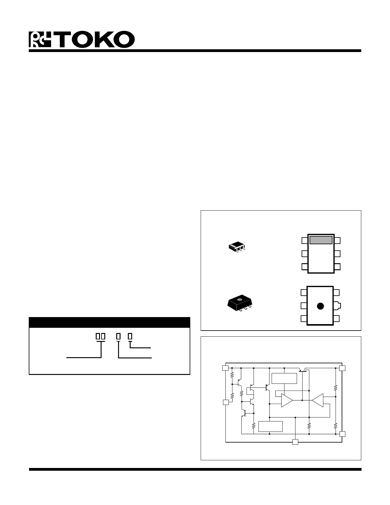
20Q
CONTROL 1
6 VIN
GND 2
5 GND
NOISE
BYPASS
3
4 VOUT
NOISE
BYPASS 1
GND 2
CONTROL 3
6 VOUT
5 GND
4 VIN
BLOCK DIAGRAM
VIN
SS
S
CONTROL
S
S SS
THERMAL
PROTECTION
–
S+
S
S
BANDGAP
REFERENCE
S
S
S
SS
S
+
–
NOISE BYPASS
S VOUT
S
S GND
Page 1
1 page 
TK113xxB
TYPICAL PERFORMANCE CHARACTERISTICS (CONT.)
TA = 25 °C unless otherwise specified
OUTPUT CURRENT vs.
QUIESCENT CURRENT
REVERSE BIAS CURRENT
(VIN = 0 V)
VIN vs. QUIESCENT CURRENT
(OFF MODE)
10 500 100
1.9 V
8 400
6 300
2.0 V
50
4 200 1.3 V
2 100
0 00
0 100 200 0
10 20 0
10 20
IO (mA)
VREV (V)
VCC (V)
VIN vs. QUIESCENT CURRENT
(ON MODE)
2 IO = 0 mA
VO =
1 3V
5V
2V 4V
VO = 1.3 to 1.8 V
0
0 5 10
VIN (V )
DROPOUT VOLTAGE
500
400
300
200
100
0
-50
IO = 150 mA
IO = 60 mA
IO = 30 mA
0 50
TA (°C)
100
May, 1997 TOKO, Inc.
VIN vs. QUIESCENT CURRENT
(ON MODE)
1.0 IO = 0 mA
VO
VO = 1.9 V
0.5
0 VO = 1.3 to 1.8 V
0 2.5 5
VIN (V)
CONTROL CURRENT
50
40
30
20
10
0
-50
VCONT = 5 V
VCONT = 1.8 V
0 50
TA (°C)
100
QUIESCENT CURRENT
2
IO = 60 mA
1
IO = 30 mA
0
-50
0 50
TA (°C)
100
VCONT (VOUT, ON POINT)
2.0 RC = 0 V
1.0
0
-50
0 50
TA (°C)
100
Page 5
5 Page 
TK113xxB
DEFINITION AND EXPLANATION OF TECHNICAL TERMS (CONT.)
PACKAGE POWER DISSIPATION (PD)
This is the power dissipation level at which the thermal sensor is activated. The IC contains an internal thermal sensor
which monitors the junction temperature. When the junction temperature exceeds the monitor threshold of 150 °C, the
IC is shutdown. The junction temperature rises as the difference between the input power (VIN X IIN) and the output power
(VOUT X IOUT) increases. The rate of temperature rise is greatly affected by the mounting pad configuration on the PCB,
the board material, and the ambient temperature. When the IC mounting has good thermal conductivity, the junction
temperature will be low even if the power dissipation is great. When mounted on the recommended mounting pad, the
power dissipation of the SOT-23L is increased to 600 mW. For operation at ambient temperatures over 25 °C, the power
dissipation of the SOT-23L device should be derated at 4.8 mW/°C. The power dissipation of the SOT-89-5 package is
900 mW when mounted as recommended. Derate the power dissipation at 7.2 mW/°C for operation above 25 °C. To
determine the power dissipation for shutdown when mounted, attach the device on the actual PCB and deliberately
increase the output current (or raise the input voltage) until the thermal protection circuit is activated. Calculate the power
dissipation of the device by subtracting the output power from the input power. These measurements should allow for the
ambient temperature of the PCB. The value obtained from PD/(150 °C - TA) is the derating factor. The PCB mounting
pad should provide maximum thermal conductivity in order to maintain low device temperatures. As a general rule, the
lower the temperature, the better the reliability of the device. The Thermal resistance when mounted is expressed as
follows:
TJ = 0JA X PD + TA
For Toko ICs, the internal limit for junction temperature is 150 °C. If the ambient temperature, TA is 25 °C, then:
150 °C = 0JA X PD + 25 °C
0JA X PD = 125 °C
0JA = 125 °C/ PD
PD is the value when the thermal sensor is activated. A simple way to determine PD is to calculate VIN X IIN when the output
side is shorted. Input current gradually falls as temperature rises. You should use the value when thermal equilibrium is
reached.
The range of currents usable can also be found from the graph below.
(mW)
PD
3
Dpd 6
4
5
Procedure:
25 50 75
150
T (°C)
1.) Find PD
2.) PD1 is taken to be PD X (≈0.8 ~ 0.9)
3.) Plot PD1 against 25 °C
4.) Connect PD1 to the point corresponding to the 150 °C with a straight line.
5.) In design, take a vertical line from the maximum operating temperature (e.g. 75 °C) to the derating curve.
6.) Read off the value of PD against the point at which the vertical line intersects the derating curve. This is taken as the
maximum power dissipation, DPD.
May, 1997 TOKO, Inc.
Page 11
11 Page | ||
| Páginas | Total 13 Páginas | |
| PDF Descargar | [ Datasheet TK11328B.PDF ] | |
Hoja de datos destacado
| Número de pieza | Descripción | Fabricantes |
| TK11328B | VOLTAGE REGULATOR WITH ON/OFF SWITCH | TOKO |
| TK11328BMCB | VOLTAGE REGULATOR WITH ON/OFF SWITCH | TOKO |
| TK11328BMCL | VOLTAGE REGULATOR WITH ON/OFF SWITCH | TOKO |
| TK11328BMIB | VOLTAGE REGULATOR WITH ON/OFF SWITCH | TOKO |
| Número de pieza | Descripción | Fabricantes |
| SLA6805M | High Voltage 3 phase Motor Driver IC. |
Sanken |
| SDC1742 | 12- and 14-Bit Hybrid Synchro / Resolver-to-Digital Converters. |
Analog Devices |
|
DataSheet.es es una pagina web que funciona como un repositorio de manuales o hoja de datos de muchos de los productos más populares, |
| DataSheet.es | 2020 | Privacy Policy | Contacto | Buscar |